
 My Inquiry
 My Account


onsemi A5191HRTNG-XTD
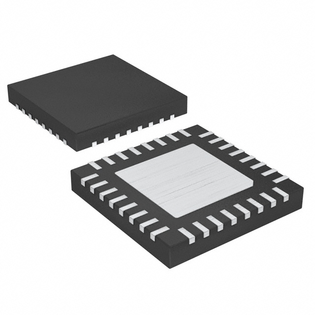
- Part No.:
- A5191HRTNG-XTD
- Manufacturer:
- onsemi
- Category:
- Modems - ICs and Modules
- Package:
- 32-VFQFN Exposed Pad
- Datasheet:
-
 A5191HRTNG-XTD.pdf
- Description:
- IC HART MODEM CMOS 32QFN
- Quantity:
- Payment:

- Shipping:

Inventory:3,768
Please send an inquiry. Send us your inquiry, and we will respond immediately.
Product details
Overview
A5191HRTNG-XTD from onsemi is a single-chip, half-duplex HART physical layer modem IC for field instrument and master applications. It implements Bell 202-compliant 1200 bps FSK modulation/demodulation at 1200 Hz and 2200 Hz, operates from 3.0 V to 5.5 V, supports industrial temperature range (−40 °C to +85 °C), and integrates receive band-pass filtering, carrier detect, and transmit-signal shaping for 4–20 mA loop-powered transmitters.
For engineers reviewing the A5191HRTNG-XTD datasheet, pinout, applications, or equivalent options, key selection considerations include its QFN-32 package with exposed pad, internal 460.8 kHz oscillator interface, dual supply architecture (VDD/VDDA), and compliance with HART physical layer timing, jitter (<12% of 1 bit), and signal amplitude thresholds (100 mVp-p carrier detect).
Technical Context
The A5191HRTNG-XTD implements phase-continuous numeric-controlled oscillator (NCO) modulation to ensure zero-phase discontinuity during mark/space transitions, enabling compliant HART waveform generation. Its demodulator uses a three-pole high-pass analog filter followed by comparator-based zero-crossing detection and carrier detect qualification logic requiring four consecutive input cycles.
It employs separate analog (VDDA/VSSA) and digital (VDD/VSS) supply domains with dedicated reference inputs (AREF, CDREF) and bias current control via external RBIAS resistor (500 kΩ typical). Carrier detect activation is set to nominal 100 mVp-p by configuring CDREF = AREF − 80 mV DC, and RTSB enables half-duplex mode switching between transmit and receive states.
Key Specifications
| Parameter | Value and Actual Design Meaning |
|---|---|
| Modulation Scheme | Phase-continuous FSK at 1200/2200 Hz per Bell 202; ensures HART-compliant spectral purity and zero-phase glitching during data transitions. |
| Data Rate | 1200 bps NRZ; matches HART protocol timing requirements and UART frame structure (1 start, 8 data, 1 odd parity, 1 stop bit). |
| Supply Voltage | 3.0 V to 5.5 V; supports direct interfacing with both 3.3 V and 5 V microcontrollers without level shifting. |
| Operating Temperature | −40 °C to +85 °C; qualified for industrial field instrumentation environments including hazardous area intrinsically safe designs. |
| Demodulator Jitter | ≤12% of 1 bit period; measured under 1200 Hz ±10 Hz / 2200 Hz ±20 Hz input, 460.8 kHz ±0.1% clock, and zero RxA asymmetry - meets HART spec margin. |
| Carrier Detect Threshold | Configurable to nominal 100 mVp-p via CDREF = AREF − 80 mV; activates CD output after four valid input cycles, rejecting sub-threshold noise. |
| Internal Clock Source | 460.8 kHz ceramic resonator or external clock on XIN/XOUT; eliminates need for precision crystal while maintaining <±1% frequency tolerance. |
Pinout & Package
Package: 32-pin QFN (5 mm × 5 mm, 0.5 mm pitch), RoHS-compliant, with exposed thermal pad connected to VSS.
| Pin/Terminal | Circuit Role | Design Meaning |
|---|---|---|
| 1 (TEST5) | Digital input | Factory test pin; must be tied to VSS for normal operation. |
| 2 (RESETB) | Digital input | Active-low reset; holds all digital logic in reset until VDD ≥ 2.5 V and tPOR ≥ 10 ns elapses. |
| 7 (TxA) | Analog output | FSK-modulated trapezoidal transmit waveform (0.25–0.75 V swing at AREF = 1.235 V); enabled only when RTSB is low. |
| 8 (AREF) | Analog input | Reference voltage (typically 1.235 V) setting DC operating point for Rx amplifier and comparator; determines CDREF offset. |
| 13 (VDDA) | Analog power | Separate 3.0–5.5 V supply for analog circuitry; decoupling required to minimize noise coupling into Rx path. |
| 14 (RxA) | Analog input | HART FSK signal input (1200/2200 Hz); accepts 80–120 mVp-p signals; connects directly to 4–20 mA loop interface. |
| 17 (XOUT) | Oscillator output | Drives external 460.8 kHz ceramic resonator (parallel mode) or receives external clock signal. |
| 22 (RTSB) | Digital input | Active-low request-to-send; controls half-duplex mode: low = transmit, high = receive; must be high at power-up. |
| 23 (TxD) | Digital input | NRZ serial data input from MCU; high = 1200 Hz (mark), low = 2200 Hz (space); synchronous with RTSB state. |
| 25 (RxD) | Digital output | Demodulated NRZ data output; valid only when CD = high; matches TxD logic polarity (high = mark). |
| 26 (CD) | Digital output | Carrier detect flag; goes high after four consecutive RxA cycles exceed threshold; gates RxD validity. |
| EP (Exposed Pad) | Thermal/Ground | Must be soldered to PCB ground plane for thermal dissipation and noise reduction in analog section. |
Key Features
| Feature | Design Value |
|---|---|
| Integrated HART Physical Layer | Fully complies with HART Foundation specifications for modulation, demodulation, filtering, carrier detect, and signal shaping - no external analog components required beyond passive RC network and resonator. |
| Low-Power Half-Duplex Operation | Dynamic power gating disables receive circuits during transmit and vice versa; IDDA ≤ 450 µA at 3.3 V, enabling intrinsically safe loop-powered designs. |
| Dual-Supply Architecture | Independent VDD (digital) and VDDA (analog) rails with separate grounds (VSS/VSSA) minimize digital switching noise coupling into sensitive analog receive path. |
| Configurable Carrier Detect | CDREF input allows precise setting of 100 mVp-p detection threshold via AREF − 80 mV DC offset, ensuring robust operation across varying loop impedances and cable lengths. |
| Flexible Clock Interface | Supports either internal 460.8 kHz ceramic resonator (low-cost, space-saving) or external clock (lower current consumption); XIN/XOUT pins configurable for either mode. |
Applications
| HART Loop-Powered Transmitter | HART Multiplexer |
|---|---|
|
Use Scenario: Integration into 4–20 mA smart field transmitter (e.g., pressure, temperature, flow sensor) where HART communication overlays analog current signal. IC Role / Device Role / Timing Role: Physical layer modem handling FSK modulation/demodulation, carrier detection, and analog filtering - bridges MCU UART to 4–20 mA loop. Use Value: Enables bidirectional digital configuration and diagnostics over legacy analog infrastructure without modifying loop wiring or power budget. |
Use Scenario: Centralized HART communication hub connecting multiple field devices to a DCS or asset management system via single RS-232/RS-485 port. IC Role / Device Role / Timing Role: HART modem per channel; manages time-division multiplexing of multiple device addresses using precise 1200 bps timing and carrier-sense arbitration. Use Value: Reduces hardware cost and board space vs. discrete solutions; supports simultaneous polling of up to 15 devices with deterministic latency. |
| HART Modem Interface Module | Industrial Process Controller HART Port |
|
Use Scenario: Standalone HART modem board used for prototyping, calibration tools, or handheld communicators interfacing with field instruments. IC Role / Device Role / Timing Role: Core modem IC providing complete physical layer functionality - replaces multi-chip solutions with single QFN-32 footprint. Use Value: Simplifies BOM, reduces layout complexity, and accelerates time-to-market for HART-enabled test equipment and service tools. |
Use Scenario: Embedded HART port in PLC or DCS I/O module enabling direct configuration and health monitoring of connected field devices. IC Role / Device Role / Timing Role: Integrated modem handling real-time HART packet framing, error detection, and loop-powered signal conditioning within controller's analog I/O ASIC subsystem. Use Value: Eliminates need for external modem ICs or optocoupled isolation interfaces; maintains full HART protocol compliance while sharing controller's power domain. |
Equivalent & Alternatives
The following parts are listed as comparable options for similar HART physical layer modem applications.
| Alternative Part | Technical Difference | Application Difference | Selection Advice |
|---|---|---|---|
| AD5700-1ACPZ-RL7 | Single-chip HART modem with integrated 4–20 mA DAC; requires external crystal (4.096 MHz) and has higher supply current (1.2 mA typical). | Targeted at fully integrated transmitter designs needing current output; not drop-in compatible due to different pinout, clock architecture, and feature set. | Select AD5700-1 if combining HART modem with 4–20 mA current loop generation in one IC; A5191HRTNG-XTD remains preferred for discrete modem-only use cases with lower power and resonator flexibility. |
| TI HART PHY (e.g., THVD8000) | RS-485/HART transceiver with integrated signal conditioning; lacks internal modem logic - requires external MCU-based software modem or companion IC. | Designed for host-side HART communication (masters), not field device modems; does not implement FSK modulation/demodulation internally. | Choose THVD8000 for master-side isolated HART interface where MCU handles protocol stack; A5191HRTNG-XTD is required for field device-side autonomous physical layer operation. |
Compared with AD5700-1ACPZ-RL7 and THVD8000, the A5191HRTNG-XTD uniquely delivers self-contained, low-power, resonator-based HART physical layer functionality in a compact QFN package - making it optimal for space-constrained, loop-powered field instruments where integration depth and power efficiency are critical.
Availability
A5191HRTNG-XTD is available at Aetrix Electronics and suitable for industrial process control, 4–20 mA loop-powered transmitters, and HART multiplexer systems requiring stable component supply and long-term lifecycle support.
Supply support for A5191HRTNG-XTD includes scheduled delivery planning, volume procurement assistance, BOM continuity management, traceable sourcing, and lifecycle availability coordination for OEM customers, industrial embedded developers, connected-device designers, and electronics production programs.
Manufacturer
onsemi (formerly ON Semiconductor) is a global semiconductor supplier specializing in energy-efficient silicon solutions for automotive, industrial, cloud, and IoT applications.
The A5191HRTNG-XTD belongs to onsemi's industrial communications product line, designed specifically to enable reliable, low-power HART connectivity in harsh industrial environments - targeting field instrumentation, process automation, and safety-critical loop-powered systems.
FAQ
What is the primary function of the A5191HRTNG-XTD in a HART system?
The A5191HRTNG-XTD serves as a complete HART physical layer modem IC, performing FSK modulation and demodulation at 1200/2200 Hz, carrier detection, receive filtering, and transmit-signal shaping. It bridges a microcontroller's UART interface to the 4–20 mA analog loop, enabling bidirectional digital communication without external analog components beyond passive elements and a 460.8 kHz resonator. The A5191HRTNG-XTD is essential for field instruments requiring autonomous, standards-compliant HART connectivity.
Does the A5191HRTNG-XTD require an external crystal or can it use a ceramic resonator?
Yes, the A5191HRTNG-XTD supports both options: it can operate with a parallel-mode 460.8 kHz ceramic resonator connected between XIN and XOUT, or with an external 460.8 kHz clock signal applied to XOUT (with XIN grounded). The ceramic resonator option simplifies design and reduces cost, while the external clock option lowers supply current. The A5191HRTNG-XTD does not require a high-precision crystal, making it suitable for cost-sensitive industrial applications where ±1% frequency tolerance is acceptable.
How does the A5191HRTNG-XTD handle half-duplex operation between transmit and receive modes?
The A5191HRTNG-XTD uses the active-low RTSB pin to control half-duplex mode: when RTSB is low, the modulator is enabled and TxA outputs the FSK signal; when RTSB is high, the modulator is disabled and the demodulator processes RxA input. Internal power gating automatically disables receive circuitry during transmit and vice versa, minimizing cross-talk and power consumption. This behavior is intrinsic to the A5191HRTNG-XTD's architecture and requires no firmware intervention beyond controlling RTSB timing per HART protocol timing constraints.
What is the role of the CDREF and AREF pins on the A5191HRTNG-XTD?
AREF sets the analog reference voltage (typically 1.235 V) for the internal operational amplifiers and comparator, defining the DC bias point for the receive path. CDREF is a dedicated input that configures the carrier detect threshold; setting CDREF = AREF − 80 mV DC establishes a nominal 100 mVp-p detection level, meeting HART specification requirements for minimum signal amplitude. Both pins must be externally decoupled, and their relationship directly determines the sensitivity and noise immunity of the A5191HRTNG-XTD's carrier detect function.
Is the A5191HRTNG-XTD suitable for intrinsically safe (IS) applications?
Yes, the A5191HRTNG-XTD is explicitly designed for intrinsically safe applications, with features including low operating current (IDDA ≤ 450 µA at 3.3 V), wide supply range (3.0 V to 5.5 V), and compatibility with loop-powered 4–20 mA architectures. Its ability to disable unused circuit blocks during transmit/receive phases further reduces peak power draw. When combined with appropriate external safety barriers and layout practices, the A5191HRTNG-XTD meets the power and thermal constraints required for IS certification in hazardous locations - a key requirement validated in its industrial temperature rating (−40 °C to +85 °C).
A5191HRTNG-XTD Specifications
- Product attributes
- Attribute value
- Manufacturer:
- onsemi
- Series:
- -
- Package/Case:
- 32-VFQFN Exposed Pad
- Packaging:
- Tube
- Product Status:
- Obsolete
- Data Format:
- HART
- Baud Rates:
- 1.2k
- Voltage - Supply:
- 3V ~ 5V
- Mounting Type:
- Surface Mount
- Supplier Device Package:
- 32-QFN (5x5)
A5191HRTNG-XTD FAQ
1.How can I place an order for A5191HRTNG-XTD through Aetrix?
Please submit a Request for Quotation (RFQ) for A5191HRTNG-XTD on Aetrix. Our sales agent will provide a competitive quotation and guide you through the order confirmation once you accept the terms.
2.Are the price and stock information for A5191HRTNG-XTD reliable?
The price and inventory of A5191HRTNG-XTD are updated periodically and may fluctuate due to market conditions. Stock and pricing data are typically refreshed every 24 hours. Quotation validity for A5191HRTNG-XTD is usually 5 days.
3.What payment methods are accepted for A5191HRTNG-XTD?
We accept Wire Transfer, PayPal, Credit Card, Western Union, MoneyGram, and Escrow for A5191HRTNG-XTD transactions.
Note: Certain payment methods may incur a processing fee.
4.How is shipping managed for A5191HRTNG-XTD?
A5191HRTNG-XTD orders can be shipped via leading logistics carriers, including DHL, UPS, FedEx, TNT, or Registered Mail.
Once your A5191HRTNG-XTD order is processed, you will receive an email with the shipment details and tracking number.
Note: Tracking information may take up to 24 hours to appear. Express delivery typically takes 3–5 business days.
5.How can I obtain technical support or documentation for A5191HRTNG-XTD?
For technical support, including A5191HRTNG-XTD datasheets, pinout diagrams, or application guidance, please contact our engineering support team. They can provide detailed documentation and assistance for your A5191HRTNG-XTD requirements.
6.How does Aetrix verify that A5191HRTNG-XTD is sourced from the original manufacturer or authorized distributors?
All A5191HRTNG-XTD products on Aetrix are procured from qualified distributors and authorized channels. Our dedicated quality assurance team conducts strict verification, including traceability checks and, if necessary, third-party testing. This ensures that A5191HRTNG-XTD meets industry standards.
7.What is the process for return or replacement of A5191HRTNG-XTD?
All A5191HRTNG-XTD units undergo pre-shipment inspection (PSI). If there is an issue with A5191HRTNG-XTD, returns or replacements are accepted under the following conditions:
1.Quantity discrepancies, incorrect items, or visible external defects (such as breakage or corrosion), acknowledged by Aetrix.
2.The issue is reported within 90 days of delivery.
3.The A5191HRTNG-XTD part is unused and in its original packaging.
Return procedure for A5191HRTNG-XTD:
1.Submit a request within 90 days.
2.Obtain a Return Material Authorization (RMA) from Aetrix.
A5191HRTNG-XTD Tags
-
CMX865AD4-TR1K
CML Micro
-
TDA5051AT/C1,518
NXP Semiconductors
-
CMX868AD2
CML Micro
-
CMX869BD2
CML Micro
-
AD5700-1ACPZ-RL7
Analog Devices Inc.
-
MX604TN-TR1K
CML Micro
-
AD5700BCPZ-R5
Analog Devices Inc.
-
MX604TN
CML Micro
-
FX604D4
CML Micro
-
MX614DW
CML Micro
-
FX614D4
CML Micro
-
AD5700-1BCPZ-RL7
Analog Devices Inc.
Tech Hub

Counterfeit components can hide behind convincing markings and passing basic function tests. This engineering reference covers source traceability, external inspection, X-ray, XRF, electrical testing, …

A practical engineering and sourcing framework covering lifecycle verification, lifetime-buy calculations, replacement qualification, supplier checks and counterfeit-risk controls.

TTL and CMOS logic families differ in thresholds, loading, output drive, power and timing. This engineering guide compares 74HC and 74HCT, calculates noise margins and checks 3.3 V/5 V compatibility.

A practical engineering guide to 3.3V and 5V logic compatibility, input thresholds, resistor dividers, translator ICs, MOSFET level shifting, I2C pull-ups, timing limits and power-sequencing risks.

The 74HC595 uses push-pull logic outputs, while the TPIC6B595 uses 50 V open-drain DMOS sinks for higher-power loads. This guide compares timing, current limits, 3.3 V interfacing, load wiring, thermal…

The 74HC595 converts serial data into eight stable parallel outputs. This guide covers pin functions, shift and storage timing, OE and MR behavior, drive-current limits, cascading, voltage compatibilit…

A technical comparison of level-sensitive latches and edge-triggered flip-flops, covering timing windows, setup and hold limits, master–slave operation, time borrowing, race-through, HDL inference and…

A D latch stores one bit while Enable controls when data can pass. This reference covers gate-level operation, truth tables, transparency, setup and hold timing, LE versus OE, common ICs and practical …

An SR latch stores one bit through cross-coupled feedback. This engineering reference covers NOR and NAND implementations, truth tables, forbidden-state recovery, gated operation, switch debouncing, fa…

Latch circuits retain one bit through feedback. This technical reference covers SR and D latches, truth tables, transparency, timing limits, latch-versus-flip-flop behavior, applications and common log…


