
 My Inquiry
 My Account


Allegro MicroSystems A6211GLJTR-T
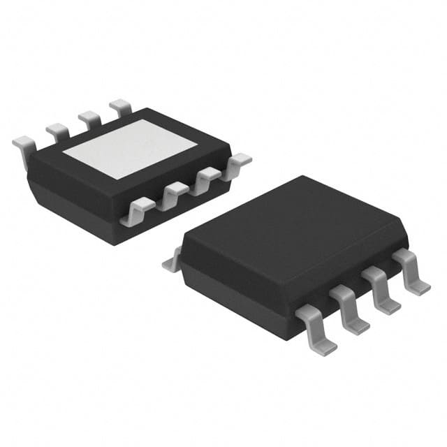
- Part No.:
- A6211GLJTR-T
- Manufacturer:
- Allegro MicroSystems
- Category:
- LED Drivers
- Package:
- 8-SOIC (0.154", 3.90mm Width) Exposed Pad
- Datasheet:
-
 A6211GLJTR-T.pdf
- Description:
- IC LED DRIVER RGLTR PWM 3A 8SOIC
- Quantity:
- Payment:

- Shipping:

Inventory:96,245
Please send an inquiry. Send us your inquiry, and we will respond immediately.
Product details
Overview
A6211GLJTR-T from Allegro MicroSystems is a constant-current, PWM-dimmable buck LED driver IC integrating a high-side N-channel DMOS switch. It delivers up to 3 A true average output current across 6–48 V input, regulates LED string voltage automatically, and supports direct logic-level PWM dimming via the EN pin. It is used in industrial lighting, MR16 display case illumination, and scanner light bars.
For engineers reviewing the A6211GLJTR-T datasheet, A6211GLJTR-T pinout, A6211GLJTR-T application, or A6211GLJTR-T equivalent, key selection criteria include its 3 A continuous output capability, cycle-by-cycle current limiting, integrated MOSFET, thermal shutdown (165°C), and SOICN-8LJ package with exposed thermal pad for PCB-level thermal management.
Technical Context
The A6211GLJTR-T employs fixed on-time, average current mode control to maintain precise LED current regulation independent of LED forward voltage variation. Its internal current sense comparator uses a 200 mV typical regulation threshold (VCSREG) referenced to the CS pin, enabling accurate current setting via external RSENSE.
Switching frequency is programmable via an external resistor (RON) between VIN and TON pins, supporting 500 kHz to 2 MHz operation. The device integrates internal loop compensation, UVLO (5.3 V threshold with 150 mV hysteresis), and robust fault protection including adjacent pin shorts, pin-to-GND shorts, and thermal shutdown with 25°C hysteresis.
Key Specifications
| Parameter | Value and Actual Design Meaning |
|---|---|
| Input Voltage Range | 6 V to 48 V - supports wide-range DC supplies including 12 V, 24 V, and 48 V industrial rails. |
| Max Output Current | 3 A - continuous true average current over –40°C to +105°C ambient, limited by thermal design. |
| Current Sense Threshold | 200 mV typical - sets LED current as iLED = 0.2 V / RSENSE; enables precise, temperature-stable regulation. |
| Switch On-Resistance | 0.25 Ω typical - reduces conduction loss at high current; impacts thermal budget and efficiency at high duty cycles. |
| UVLO Threshold | 5.3 V with 150 mV hysteresis - prevents erratic startup during brown-out; ensures clean enable/disable sequencing. |
| Thermal Shutdown | 165°C junction temperature - protects silicon under overload or poor heatsinking; 25°C hysteresis prevents cycling. |
| PWM Dimming Range | 100 Hz to 2 kHz - compatible with standard microcontroller GPIO outputs; supports ≥1% dimming ratio at 200 Hz. |
Pinout & Package
Package: 8-pin narrow SOIC (SOICN) with exposed thermal pad (suffix LJ); RoHS-compliant, lead-free, 100% matte-tin leadframe plating. Thermal pad must be soldered to PCB ground plane for optimal RθJP = 2°C/W performance.
| Pin/Terminal | Circuit Role | Design Meaning |
|---|---|---|
| VIN | Supply input | Accepts 6–48 V DC; powers internal circuitry and high-side switch; requires local ceramic + bulk capacitance. |
| TON | On-time programming | Resistor-connected node that sets switching frequency (500 kHz–2 MHz); determines tON via RON. |
| EN | Enable / PWM input | Logic-compatible (VIH = 1.8 V, VIL = 0.4 V); directly accepts PWM signals for brightness control or shutdown. |
| CS | Current sense feedback | Monitors voltage across external RSENSE; regulates average LED current to 200 mV reference. |
| VCC | Internal LDO output | 5.4 V regulated supply for gate drive and logic; not intended for external loading (max 5 mA). |
| GND | Power and signal ground | Common return for VIN, CS, EN, BOOT, SW; must be low-impedance and tied to exposed thermal pad. |
| BOOT | Bootstrap capacitor terminal | Drives high-side MOSFET gate; requires 0.1 µF ceramic capacitor between BOOT and SW pins. |
| SW | Switch node | High-di/dt connection to inductor and Schottky diode; routing must minimize loop area to reduce EMI. |
| PAD | Exposed thermal pad | Internally connected to GND; mandatory solder connection to PCB ground plane for thermal dissipation. |
Key Features
| Feature | Design Value |
|---|---|
| Integrated high-side DMOS switch | Eliminates external MOSFET and associated gate-drive complexity; reduces BOM count and layout area. |
| True average current regulation | Maintains consistent LED brightness across temperature and forward-voltage drift without optical feedback. |
| Cycle-by-cycle current limiting | Trips at 3.0–5.0 A (typical 4.0 A) to protect against shorted LEDs or inductor saturation faults. |
| Low-power shutdown mode | 1 µA typical quiescent current when EN is low - enables energy-efficient standby in battery-powered lighting. |
| Robust fault protection suite | Detects and responds to pin-to-GND shorts, adjacent pin shorts, open/short components, and missing diode conditions. |
Applications
| Industrial Lighting | Architectural Lighting |
|---|---|
Use Scenario: High-bay LED fixtures in warehouses and factories requiring stable 3 A drive for multi-LED strings. IC Role / Device Role / Timing Role: Constant-current buck regulator providing regulated current and PWM dimming interface for DALI or 0–10 V controllers. Use Value: Enables >90% efficiency at 2 A output with minimal external components; thermal pad supports convection-cooled metal-core PCBs. |
Use Scenario: Linear LED strips and cove lighting systems where color consistency and flicker-free dimming are critical. IC Role / Device Role / Timing Role: Primary current controller implementing analog or PWM dimming per zone, with automatic VOUT adjustment for varying LED counts. Use Value: Delivers <1% current ripple at 200 Hz PWM with optional 0.68 µF output capacitor; avoids visible flicker in slow-motion video capture. |
| Scanner Light Bars | MR16 Display Case Lighting |
Use Scenario: High-intensity linear light sources in document scanners and multifunction printers requiring fast PWM response. IC Role / Device Role / Timing Role: LED driver with sub-130 µs startup delay and no latency during PWM transitions - essential for synchronized image capture. Use Value: Maintains full LED current regulation during rapid 2%–100% duty-cycle changes; eliminates brightness overshoot or undershoot. |
Use Scenario: Replacement MR16 retrofit lamps operating from 12 V AC/DC with tight thermal constraints in enclosed fixtures. IC Role / Device Role / Timing Role: Compact, thermally optimized LED driver enabling 3 A output in SOICN-8LJ footprint - fits within standard MR16 housing. Use Value: Exposed thermal pad achieves RθJA = 35°C/W on 4-layer PCB, allowing full 3 A output at 105°C ambient without derating. |
Equivalent & Alternatives
The following parts are listed as comparable options for similar constant-current buck LED driver applications.
| Alternative Part | Technical Difference | Application Difference | Selection Advice |
|---|---|---|---|
| LM3409MH/NOPB | External N-MOSFET required; no integrated switch; 1.25 V current sense threshold vs. A6211GLJTR-T's 0.2 V. | Higher BOM cost and layout complexity; better suited for >5 A designs where discrete FET optimization is needed. | Select LM3409MH/NOPB only when higher output current (>3.5 A) or custom MOSFET selection is required. |
| MPQ4425AGU-AEC1-P | Automotive-grade AEC-Q100 qualified; 2.5 A max output; 0.1 V current sense threshold; requires external compensation. | Targeted at automotive interior lighting; lacks A6211GLJTR-T's integrated thermal pad and pin-level fault diagnostics. | Choose MPQ4425AGU-AEC1-P only for automotive programs requiring AEC-Q100 compliance and lower current (≤2.5 A). |
Compared with LM3409MH/NOPB and MPQ4425AGU-AEC1-P, the A6211GLJTR-T offers the highest integration (integrated 3 A switch, thermal pad, and comprehensive fault reporting) in a compact SOICN-8LJ package, making it optimal for space-constrained industrial and commercial lighting where board area and thermal performance are prioritized over automotive qualification or ultra-high current.
Availability
A6211GLJTR-T is available at Aetrix Electronics and suitable for industrial lighting, architectural lighting, and scanner light bar applications requiring stable component supply, long-term production continuity, and RoHS-compliant packaging.
Supply support for A6211GLJTR-T includes scheduled delivery planning, volume procurement assistance, BOM continuity management, traceable sourcing, and lifecycle availability coordination for OEM customers, industrial embedded developers, connected-device designers, and electronics production programs.
Manufacturer
Allegro MicroSystems is a U.S.-based semiconductor company specializing in high-performance power ICs, magnetic sensors, and motor driver solutions for automotive and industrial markets.
The A6211GLJTR-T belongs to Allegro's constant-current LED driver product line, designed specifically for high-efficiency, thermally robust, and fault-tolerant illumination systems in demanding non-automotive environments.
FAQ
What is the maximum continuous output current of the A6211GLJTR-T?
The A6211GLJTR-T delivers up to 3 A true average output current across its full operating ambient temperature range of –40°C to +105°C. This rating assumes proper PCB thermal design - specifically, connection of the exposed thermal pad to a sufficient copper area to achieve ≤35°C/W junction-to-ambient thermal resistance. At higher ambient temperatures or reduced copper area, output current must be derated per the thermal budgeting guidelines in the datasheet.
How is LED current set on the A6211GLJTR-T?
LED current on the A6211GLJTR-T is set by an external current sense resistor (RSENSE) connected between the CS pin and LED–. The device regulates the voltage at the CS pin to a typical 200 mV threshold, so iLED = 0.2 V / RSENSE. For example, a 0.15 Ω resistor sets 1.33 A output. The CS pin bias current is only 0.9 µA, minimizing error due to resistor self-heating or trace resistance.
Can the A6211GLJTR-T operate without an output capacitor across the LED string?
Yes, the A6211GLJTR-T is explicitly designed to operate without an output filter capacitor across the LED string - reducing BOM cost and board space. However, adding a small ceramic capacitor (e.g., 0.68 µF) between LED+ and LED– lowers LED current ripple and improves flicker performance. Note: placing capacitance between LED+ and GND is prohibited, as it destabilizes the current regulation loop by attenuating the required CS pin ripple.
What protection features does the A6211GLJTR-T include?
The A6211GLJTR-T integrates multiple hardware-based protections: undervoltage lockout (5.3 V threshold), thermal shutdown (165°C), cycle-by-cycle overcurrent limiting (trip at ~4 A), and robust fault detection for pin-to-GND shorts, adjacent pin shorts, open/short external components, and missing Schottky diodes. These functions operate autonomously without software intervention and trigger automatic retry after a cool-down period.
Is the A6211GLJTR-T pin-compatible with other Allegro LED drivers?
No, the A6211GLJTR-T has a unique pinout optimized for its integrated high-side switch and thermal pad configuration. It is not pin-compatible with Allegro's A6260 or A6261 families, which use different packages (e.g., 10-pin MSOP) and feature sets (e.g., analog dimming only). Migration requires PCB layout revision and revalidation of current sense, TON, and bootstrap networks.
A6211GLJTR-T Specifications
- Product attributes
- Attribute value
- Manufacturer:
- Allegro MicroSystems
- Series:
- -
- Package/Case:
- 8-SOIC (0.154", 3.90mm Width) Exposed Pad
- Packaging:
- Tape & Reel (TR)
- Product Status:
- Active
- Type:
- DC DC Regulator
- Topology:
- Step-Down (Buck)
- Internal Switch(s):
- Yes
- Number of Outputs:
- 1
- Voltage - Supply (Min):
- 6V
- Voltage - Supply (Max):
- 48V
- Voltage - Output:
- -
- Current - Output / Channel:
- 3A
- Frequency:
- -
- Dimming:
- PWM
- Applications:
- Lighting
- Operating Temperature:
- -40°C ~ 105°C (TA)
- Grade:
- -
- Qualification:
- -
- Mounting Type:
- Surface Mount
- Supplier Device Package:
- 8-SOIC-EP
A6211GLJTR-T FAQ
1.How can I place an order for A6211GLJTR-T through Aetrix?
Please submit a Request for Quotation (RFQ) for A6211GLJTR-T on Aetrix. Our sales agent will provide a competitive quotation and guide you through the order confirmation once you accept the terms.
2.Are the price and stock information for A6211GLJTR-T reliable?
The price and inventory of A6211GLJTR-T are updated periodically and may fluctuate due to market conditions. Stock and pricing data are typically refreshed every 24 hours. Quotation validity for A6211GLJTR-T is usually 5 days.
3.What payment methods are accepted for A6211GLJTR-T?
We accept Wire Transfer, PayPal, Credit Card, Western Union, MoneyGram, and Escrow for A6211GLJTR-T transactions.
Note: Certain payment methods may incur a processing fee.
4.How is shipping managed for A6211GLJTR-T?
A6211GLJTR-T orders can be shipped via leading logistics carriers, including DHL, UPS, FedEx, TNT, or Registered Mail.
Once your A6211GLJTR-T order is processed, you will receive an email with the shipment details and tracking number.
Note: Tracking information may take up to 24 hours to appear. Express delivery typically takes 3–5 business days.
5.How can I obtain technical support or documentation for A6211GLJTR-T?
For technical support, including A6211GLJTR-T datasheets, pinout diagrams, or application guidance, please contact our engineering support team. They can provide detailed documentation and assistance for your A6211GLJTR-T requirements.
6.How does Aetrix verify that A6211GLJTR-T is sourced from the original manufacturer or authorized distributors?
All A6211GLJTR-T products on Aetrix are procured from qualified distributors and authorized channels. Our dedicated quality assurance team conducts strict verification, including traceability checks and, if necessary, third-party testing. This ensures that A6211GLJTR-T meets industry standards.
7.What is the process for return or replacement of A6211GLJTR-T?
All A6211GLJTR-T units undergo pre-shipment inspection (PSI). If there is an issue with A6211GLJTR-T, returns or replacements are accepted under the following conditions:
1.Quantity discrepancies, incorrect items, or visible external defects (such as breakage or corrosion), acknowledged by Aetrix.
2.The issue is reported within 90 days of delivery.
3.The A6211GLJTR-T part is unused and in its original packaging.
Return procedure for A6211GLJTR-T:
1.Submit a request within 90 days.
2.Obtain a Return Material Authorization (RMA) from Aetrix.
A6211GLJTR-T Tags

-
BCR402RE6327HTSA1
Infineon Technologies

-
BCR430UXTSA2
Infineon Technologies

-
BCR420UE6433HTMA1
Infineon Technologies
-
BCR420UE6327HTSA1
Infineon Technologies
-
BCR421UE6327HTSA1
Infineon Technologies

-
LYT1604D-TL
Power Integrations

-
HV9910CLG-G
Microchip Technology

-
CL2N8-G
Microchip Technology

-
BCR420UW6-7
Diodes Incorporated
-
BCR421UW6-7
Diodes Incorporated

-
BCR420UFD-7
Diodes Incorporated
-
BCR421UFD-7
Diodes Incorporated
Tech Hub

A practical engineering and sourcing framework covering lifecycle verification, lifetime-buy calculations, replacement qualification, supplier checks and counterfeit-risk controls.

TTL and CMOS logic families differ in thresholds, loading, output drive, power and timing. This engineering guide compares 74HC and 74HCT, calculates noise margins and checks 3.3 V/5 V compatibility.

A practical engineering guide to 3.3V and 5V logic compatibility, input thresholds, resistor dividers, translator ICs, MOSFET level shifting, I2C pull-ups, timing limits and power-sequencing risks.

The 74HC595 uses push-pull logic outputs, while the TPIC6B595 uses 50 V open-drain DMOS sinks for higher-power loads. This guide compares timing, current limits, 3.3 V interfacing, load wiring, thermal…

The 74HC595 converts serial data into eight stable parallel outputs. This guide covers pin functions, shift and storage timing, OE and MR behavior, drive-current limits, cascading, voltage compatibilit…

A technical comparison of level-sensitive latches and edge-triggered flip-flops, covering timing windows, setup and hold limits, master–slave operation, time borrowing, race-through, HDL inference and…

A D latch stores one bit while Enable controls when data can pass. This reference covers gate-level operation, truth tables, transparency, setup and hold timing, LE versus OE, common ICs and practical …

An SR latch stores one bit through cross-coupled feedback. This engineering reference covers NOR and NAND implementations, truth tables, forbidden-state recovery, gated operation, switch debouncing, fa…

Latch circuits retain one bit through feedback. This technical reference covers SR and D latches, truth tables, transparency, timing limits, latch-versus-flip-flop behavior, applications and common log…

An engineering guide to LED driver operation, constant-current and constant-voltage outputs, linear and switching topologies, dimming, IC selection, calculations, replacement compatibility, and fault c…


