
 My Inquiry
 My Account


Allegro MicroSystems A6280EESTR-T
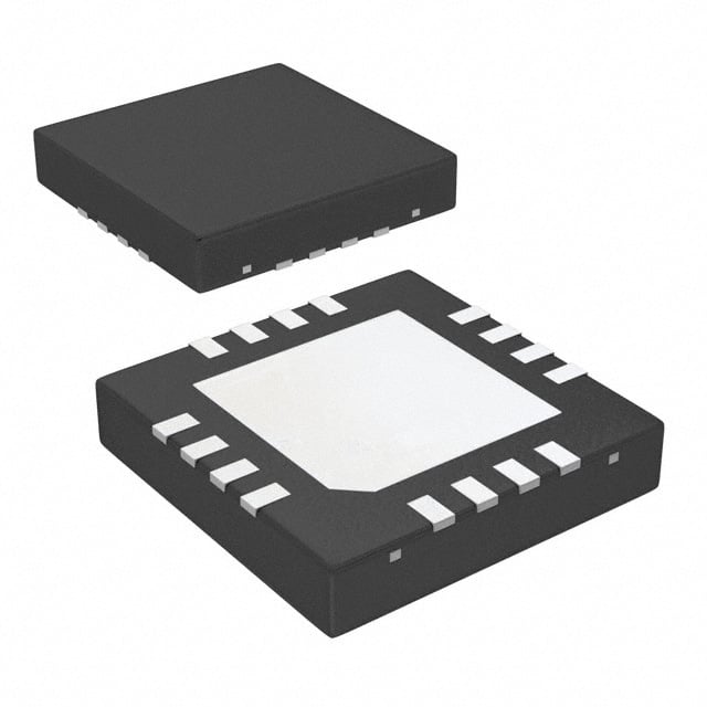
- Part No.:
- A6280EESTR-T
- Manufacturer:
- Allegro MicroSystems
- Category:
- LED Drivers
- Package:
- 16-WFQFN Exposed Pad
- Datasheet:
-
 A6280EESTR-T.pdf
- Description:
- IC LED DRVR LIN PWM 150MA 16QFN
- Quantity:
- Payment:

- Shipping:

Inventory:3,709
Please send an inquiry. Send us your inquiry, and we will respond immediately.
Product details
Overview
A6280EESTR-T from Allegro MicroSystems is a 3-channel constant-current LED driver IC designed for RGB pixel control in large-character signage and architectural lighting. It delivers programmable 10-bit PWM brightness per channel (0–1023 levels), 7-bit dot correction per output, and supports 10–150 mA output current per channel via external REXT. The device operates from 5–17 V and enables daisy-chained control of hundreds of LEDs using only four logic signals.
For engineers reviewing the A6280EESTR-T datasheet, A6280EESTR-T pinout, A6280EESTR-T application, or A6280EESTR-T equivalent, key selection considerations include its QFN-16 package, shared serial/PWM clock pin architecture, thermal shutdown (165°C), undervoltage lockout (3.0–4.5 V), and compatibility with high-speed daisy-chain topologies requiring precise CI-to-LI setup timing.
Technical Context
The A6280EESTR-T integrates three independent linear current regulators with matched output characteristics (±7% matching error) and embeds a 31-bit shift register that loads brightness, dot correction, and clock divider data via SDI/CI. Its dual-function CI pin concurrently serves as serial clock input and PWM timing source, reducing pin count while enabling synchronized daisy chaining.
Each channel features a dedicated 10-bit PWM counter and 7-bit scalar register; brightness data determines duty cycle (DC = [(PWMn + 1)/1024] × 100%), while dot correction scales maximum current from 36.5% to 100% to compensate for LED binning and aging. Internal thermal shutdown and UVLO protect against overtemperature and supply brownout.
Key Specifications
| Parameter | Value and Actual Design Meaning |
|---|---|
| Output channels | 3 independent sinking outputs (OUT0, OUT1, OUT2) for RGB LED control |
| Max output current | 150 mA per channel at REXT = 5 kΩ; adjustable down to 10 mA via REXT |
| Brightness resolution | 10-bit per channel → 1024 discrete intensity levels (0% to 100% duty cycle) |
| Dot correction | 7-bit per channel → 128 scaling steps from 36.5% to 100% of max current |
| Supply voltage range | 5.0–17 V on VIN; internal regulator powers logic from same rail |
| Logic interface speed | Serial clock (CI) up to 5 MHz; buffered CO/SDO/LO/OEO support >250-device chains |
| Thermal protection | Thermal shutdown at 165°C typical; 15°C hysteresis ensures stable recovery |
| UVLO threshold | 3.0–4.0 V falling edge; 3.5–4.5 V rising edge - prevents erratic output during brownout |
Pinout & Package
Package: 16-contact QFN (ES suffix), lead-free with 100% matte-tin plating; exposed thermal pad (PAD) must be externally connected to LGND and PGND for thermal performance.
| Pin/Terminal | Circuit Role | Design Meaning |
|---|---|---|
| OUT0 / OUT1 / OUT2 | Sinking LED current output | Three independent constant-current sinks; each drives one LED anode via common cathode |
| REXT | Current reference input | External resistor sets global max current: IOUT(max) = 753.12 / REXT (kΩ → mA) |
| VREG | Internal regulator decoupling | Requires 1.0 μF ceramic capacitor to LGND; not an output supply rail |
| VIN | Chip power supply | Supplies both logic and output drivers; connects directly to LED bus (no separate chip rail needed) |
| CI | Shared serial clock / PWM clock input | Rising edge clocks shift register; falling edge updates SDO; also drives internal PWM counter when OEI low |
| SDI / SDO | Serial data in/out | FIFO-shifted 31-bit register: bit 30 selects address mode (brightness vs dot correction/clock divider) |
| LI / LO | Latch input/output | Rising edge latches shift register contents; LO drives next device's LI - enables chain synchronization |
| OEI / OEO | Output enable input/output | Active-low OEI enables all outputs; OEO propagates signal downstream for global blanking |
| LGND / PGND | Logic / power ground | Separate ground paths minimize noise coupling; both must connect to exposed PAD |
Key Features
| Feature | Design Value |
|---|---|
| 3 × 10-bit PWM registers | Enables 1.07 billion RGB color combinations (1024³) without external microcontroller PWM generation |
| 3 × 7-bit dot correction scalars | Compensates for LED forward-voltage mismatch and aging drift to maintain white-point stability across panels |
| Shared CI pin for serial + PWM clock | Reduces system pin count and eliminates need for separate timing sources - simplifies controller interface |
| Buffered chain outputs (CO/LO/OEO/SDO) | Drives >250 devices in series over Cat5 UTP without signal degradation or duty-cycle skew |
| Integrated linear regulator | Eliminates external 5 V regulator; allows VIN to tie directly to LED supply bus (5–17 V) |
| Thermal shutdown + UVLO | Prevents latch-up or thermal runaway in high-density signage; preserves latch data during fault events |
Applications
| Colored Large-Character LED Signs | Architectural Lighting |
|---|---|
|
Use Scenario: Outdoor alphanumeric displays with wide viewing angles and high ambient light rejection. IC Role / Device Role / Timing Role: Constant-current sink for red/green/blue LED clusters; PWM brightness control synchronizes color blending across 100+ characters. Use Value: 10-bit PWM resolution ensures smooth grayscale transitions; dot correction maintains consistent chromaticity across large panel areas despite LED batch variation. |
Use Scenario: Facade illumination with dynamic color-changing effects on building exteriors. IC Role / Device Role / Timing Role: Distributed current driver in daisy-chained pixel modules; buffered CO/LO/OEO signals maintain timing integrity over 30+ meter cable runs. Use Value: Shared CI pin architecture reduces controller I/O count; thermal shutdown protects against enclosure overheating in sealed fixtures. |
| Scrolling Colored Marquees | High-Intensity Monochrome Displays |
|
Use Scenario: Highway-facing message boards requiring high brightness (>8000 cd/m²) and reliable 24/7 operation. IC Role / Device Role / Timing Role: Primary LED current controller with programmable dot correction to offset LED aging over 50,000-hour lifespan. Use Value: 7-bit dot correction enables field recalibration of luminance uniformity without hardware modification. |
Use Scenario: Emergency exit signage and industrial status indicators using high-luminance amber or white LEDs. IC Role / Device Role / Timing Role: Single-channel current regulator (using only OUT0) with full 150 mA capability and thermal foldback. Use Value: Wide 5–17 V input range accommodates battery-backed or PoE-powered installations; UVLO prevents flicker during brownout conditions. |
Equivalent & Alternatives
The following parts are listed as comparable options for similar 3-channel constant-current LED driver applications.
| Alternative Part | Technical Difference | Application Difference | Selection Advice |
|---|---|---|---|
| TLC59284PWR | 16-bit PWM resolution; no integrated dot correction; requires external current-setting resistors per channel | Higher grayscale fidelity but lacks per-channel current trimming - less suitable for mixed-bin LED arrays | Preferred for precision grayscale applications where LED matching is tightly controlled at board level |
| MAX6967AUG+T | I²C interface (not SPI-compatible); 8-bit PWM + 6-bit current control; integrated open/short LED detection | Lower pin count but limited to ~16 devices per bus; no daisy-chain capability - unsuitable for large signage | Best for compact, low-channel-count designs requiring diagnostics and minimal MCU GPIO usage |
Compared with TLC59284PWR and MAX6967AUG+T, the A6280EESTR-T uniquely balances daisy-chain scalability, per-channel dot correction, and shared-clock efficiency - making it optimal for large-format RGB signage where uniformity and wiring simplicity are critical.
Availability
A6280EESTR-T is available at Aetrix Electronics and suitable for colored large-character LED signs, architectural lighting, and scrolling marquees requiring stable component supply during legacy design support and end-of-life transition phases.
Supply support for A6280EESTR-T includes scheduled delivery planning, volume procurement assistance, BOM continuity management, traceable sourcing, and lifecycle availability coordination for OEM customers, industrial embedded developers, connected-device designers, and electronics production programs.
Manufacturer
Allegro MicroSystems is a U.S.-based designer of high-performance magnetic sensing and power IC solutions, headquartered in Worcester, Massachusetts.
The A6280 product line was developed specifically for high-reliability, large-pixel-count LED display systems requiring precise current matching, thermal robustness, and scalable serial control - targeting outdoor signage and architectural applications.
FAQ
What is the function of the REXT pin on the A6280EESTR-T?
The REXT pin on the A6280EESTR-T accepts an external resistor that sets the global maximum output current for all three channels using the formula IOUT(max) = 753.12 / REXT. For example, a 5 kΩ resistor yields ~150 mA per channel. This resistor establishes a stable current reference independent of supply voltage, temperature, or LED VF variation - ensuring consistent brightness across operating conditions. The A6280EESTR-T uses this value as the baseline for all dot correction and PWM scaling operations.
How does the A6280EESTR-T support daisy-chaining of multiple devices?
The A6280EESTR-T supports daisy-chaining through buffered outputs: CO (Clock Out), LO (Latch Out), OEO (Output Enable Out), and SDO (Serial Data Out) replicate their respective inputs (CI, LI, OEI, SDI) with TTL-level drive strength. These outputs drive the next device's inputs directly, enabling chains of up to 250+ units over Cat5 UTP. The internal 100 ns one-shot on CO ensures clock edge consistency across the chain, while the 31-bit shift register and address-bit protocol prevent data corruption during long serial transfers - a core capability of the A6280EESTR-T.
What is the purpose of the dual-mode shift register in the A6280EESTR-T?
The A6280EESTR-T's 31-bit shift register uses bit 30 as an address selector: when '0', subsequent bits load into the three 10-bit PWM brightness registers; when '1', they load into dot correction and clock divider configuration fields. This dual-mode architecture allows full control of both intensity and current scaling using a single serial interface - eliminating the need for separate command protocols or additional control lines. This design directly enables the A6280EESTR-T's compact 16-pin QFN footprint while retaining full functional flexibility.
Does the A6280EESTR-T require an external voltage regulator?
No, the A6280EESTR-T integrates an internal linear regulator that derives logic power from the VIN supply (5–17 V), eliminating the need for an external 5 V regulator. The VREG pin is solely for decoupling - a 1.0 μF ceramic capacitor must connect between VREG and LGND. When VIN is 5 V, it must be externally tied to VREG to ensure proper regulation; however, VIN must never exceed the VREG absolute maximum rating of 6 V. This integrated regulation is a defining feature of the A6280EESTR-T, simplifying power architecture in LED pixel boards.
What happens to the A6280EESTR-T outputs during thermal shutdown?
When the A6280EESTR-T junction temperature reaches 165°C (typical), thermal shutdown disables all three output drivers (OUT0/OUT1/OUT2) until the die cools by ~15°C. Crucially, the shift register, latch registers, and logic circuitry remain fully operational - preserving all loaded brightness, dot correction, and clock divider settings. Once temperature falls below the recovery threshold (~150°C), outputs resume normal operation using the retained configuration. This behavior ensures display state integrity during transient overtemperature events - a critical reliability feature of the A6280EESTR-T in enclosed or high-power-density signage.
A6280EESTR-T Specifications
- Product attributes
- Attribute value
- Manufacturer:
- Allegro MicroSystems
- Series:
- -
- Package/Case:
- 16-WFQFN Exposed Pad
- Packaging:
- Tape & Reel (TR)
- Product Status:
- Obsolete
- Type:
- Linear
- Topology:
- Shift Register
- Internal Switch(s):
- Yes
- Number of Outputs:
- 3
- Voltage - Supply (Min):
- 4.75V
- Voltage - Supply (Max):
- 17V
- Voltage - Output:
- 1V ~ 3V
- Current - Output / Channel:
- 150mA
- Frequency:
- 5MHz
- Dimming:
- PWM
- Applications:
- Lighting
- Operating Temperature:
- -40°C ~ 85°C (TA)
- Grade:
- -
- Qualification:
- -
- Mounting Type:
- Surface Mount
- Supplier Device Package:
- 16-QFN/MLP (3x3)
A6280EESTR-T FAQ
1.How can I place an order for A6280EESTR-T through Aetrix?
Please submit a Request for Quotation (RFQ) for A6280EESTR-T on Aetrix. Our sales agent will provide a competitive quotation and guide you through the order confirmation once you accept the terms.
2.Are the price and stock information for A6280EESTR-T reliable?
The price and inventory of A6280EESTR-T are updated periodically and may fluctuate due to market conditions. Stock and pricing data are typically refreshed every 24 hours. Quotation validity for A6280EESTR-T is usually 5 days.
3.What payment methods are accepted for A6280EESTR-T?
We accept Wire Transfer, PayPal, Credit Card, Western Union, MoneyGram, and Escrow for A6280EESTR-T transactions.
Note: Certain payment methods may incur a processing fee.
4.How is shipping managed for A6280EESTR-T?
A6280EESTR-T orders can be shipped via leading logistics carriers, including DHL, UPS, FedEx, TNT, or Registered Mail.
Once your A6280EESTR-T order is processed, you will receive an email with the shipment details and tracking number.
Note: Tracking information may take up to 24 hours to appear. Express delivery typically takes 3–5 business days.
5.How can I obtain technical support or documentation for A6280EESTR-T?
For technical support, including A6280EESTR-T datasheets, pinout diagrams, or application guidance, please contact our engineering support team. They can provide detailed documentation and assistance for your A6280EESTR-T requirements.
6.How does Aetrix verify that A6280EESTR-T is sourced from the original manufacturer or authorized distributors?
All A6280EESTR-T products on Aetrix are procured from qualified distributors and authorized channels. Our dedicated quality assurance team conducts strict verification, including traceability checks and, if necessary, third-party testing. This ensures that A6280EESTR-T meets industry standards.
7.What is the process for return or replacement of A6280EESTR-T?
All A6280EESTR-T units undergo pre-shipment inspection (PSI). If there is an issue with A6280EESTR-T, returns or replacements are accepted under the following conditions:
1.Quantity discrepancies, incorrect items, or visible external defects (such as breakage or corrosion), acknowledged by Aetrix.
2.The issue is reported within 90 days of delivery.
3.The A6280EESTR-T part is unused and in its original packaging.
Return procedure for A6280EESTR-T:
1.Submit a request within 90 days.
2.Obtain a Return Material Authorization (RMA) from Aetrix.
A6280EESTR-T Tags

-
BCR402RE6327HTSA1
Infineon Technologies

-
BCR430UXTSA2
Infineon Technologies

-
BCR420UE6433HTMA1
Infineon Technologies
-
BCR420UE6327HTSA1
Infineon Technologies
-
BCR421UE6327HTSA1
Infineon Technologies

-
LYT1604D-TL
Power Integrations

-
HV9910CLG-G
Microchip Technology

-
CL2N8-G
Microchip Technology

-
BCR420UW6-7
Diodes Incorporated
-
BCR421UW6-7
Diodes Incorporated

-
BCR420UFD-7
Diodes Incorporated
-
BCR421UFD-7
Diodes Incorporated
Tech Hub

A practical engineering and sourcing framework covering lifecycle verification, lifetime-buy calculations, replacement qualification, supplier checks and counterfeit-risk controls.

TTL and CMOS logic families differ in thresholds, loading, output drive, power and timing. This engineering guide compares 74HC and 74HCT, calculates noise margins and checks 3.3 V/5 V compatibility.

A practical engineering guide to 3.3V and 5V logic compatibility, input thresholds, resistor dividers, translator ICs, MOSFET level shifting, I2C pull-ups, timing limits and power-sequencing risks.

The 74HC595 uses push-pull logic outputs, while the TPIC6B595 uses 50 V open-drain DMOS sinks for higher-power loads. This guide compares timing, current limits, 3.3 V interfacing, load wiring, thermal…

The 74HC595 converts serial data into eight stable parallel outputs. This guide covers pin functions, shift and storage timing, OE and MR behavior, drive-current limits, cascading, voltage compatibilit…

A technical comparison of level-sensitive latches and edge-triggered flip-flops, covering timing windows, setup and hold limits, master–slave operation, time borrowing, race-through, HDL inference and…

A D latch stores one bit while Enable controls when data can pass. This reference covers gate-level operation, truth tables, transparency, setup and hold timing, LE versus OE, common ICs and practical …

An SR latch stores one bit through cross-coupled feedback. This engineering reference covers NOR and NAND implementations, truth tables, forbidden-state recovery, gated operation, switch debouncing, fa…

Latch circuits retain one bit through feedback. This technical reference covers SR and D latches, truth tables, transparency, timing limits, latch-versus-flip-flop behavior, applications and common log…

An engineering guide to LED driver operation, constant-current and constant-voltage outputs, linear and switching topologies, dimming, IC selection, calculations, replacement compatibility, and fault c…


