
 My Inquiry
 My Account


Allegro MicroSystems A80603KESJSR-1
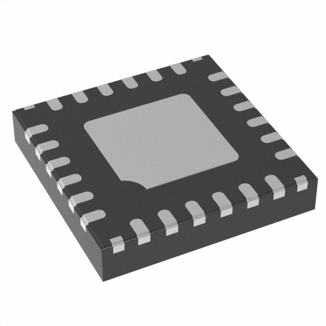
- Part No.:
- A80603KESJSR-1
- Manufacturer:
- Allegro MicroSystems
- Category:
- LED Drivers
- Package:
- 24-WFQFN Exposed Pad
- Datasheet:
-
 A80603KESJSR-1.pdf
- Description:
- IC LED DRVR CTRL PWM 120MA 24QFN
- Quantity:
- Payment:

- Shipping:

Inventory:2,362
Please send an inquiry. Send us your inquiry, and we will respond immediately.
Product details
Overview
A80603KESJSR-1 from Allegro MicroSystems is an AEC-Q100 qualified automotive LED driver IC integrating a current-mode boost converter with internal 250 mΩ NMOS switch and four precision current sinks. It delivers up to 120 mA per string across 4 parallel channels (480 mA total), operates from 4.5–40 V input, and achieves 15,000:1 PWM dimming contrast ratio at 200 Hz in infotainment backlighting systems.
For engineers reviewing the A80603KESJSR-1 datasheet, A80603KESJSR-1 pinout, A80603KESJSR-1 application, or A80603KESJSR-1 equivalent, this page provides verified technical context, validated pin functions, confirmed automotive-grade protection features, and real-world design implications for stop/start and load-dump resilient lighting systems.
Technical Context
The A80603KESJSR-1 implements Pre-Emptive Boost (PEB) control to minimize output ripple and enable sub-0.3 µs minimum PWM on-time-critical for eliminating MLCC audible noise in automotive displays. Its dual-mode operation supports both boost and SEPIC topologies, with programmable switching frequency (260 kHz–2.3 MHz) via resistor or external sync, plus dithering for EMI reduction.
It integrates fault detection for LED open/short, boost switch overcurrent (3.75 A primary limit), input UVLO (3.95 V stop threshold), thermal shutdown (170 °C), and OVP latch (55 V at SW). The FAULT pin behavior differs from A80603: A80603KESJSR-1 releases FAULT at the start of LED detection phase and uses a 16 ms soft-start timer.
Key Specifications
| Parameter | Value and Actual Design Meaning |
|---|---|
| Input Voltage Range | 4.5–40 V startup; sustains operation down to 3.9 V-enables robust cold-crank and load-dump survival in 12 V automotive systems. |
| LED Current Accuracy | ±0.7% typical per channel-ensures uniform brightness across 4 strings without external calibration. |
| PWM Dimming Ratio | 15,000:1 at 200 Hz (PWM-only); 150,000:1 with combined PWM + APWM-meets ASIL B display contrast requirements. |
| Switching Frequency | 260 kHz–2.3 MHz, resistor- or sync-programmable-allows AM-band avoidance and EMI optimization. |
| Thermal Resistance | RθJA = 37 °C/W on 4-layer JEDEC board-supports continuous 480 mA output with standard PCB thermal relief. |
| Soft-Start Time | 16 ms (A80603KESJSR-1 specific)-slower ramp than A80603 (8 ms) improves inrush control in high-capacitance LED arrays. |
| AEC-Q100 Grade | Qualified to Grade 1 (–40 °C to +125 °C ambient)-validates operation in instrument cluster and center stack environments. |
Pinout & Package
24-pin 4 mm × 4 mm QFN with wettable flank and exposed thermal pad. Requires ≥8 vias to ground plane for thermal reliability in automotive power dissipation scenarios.
| Pin/Terminal | Circuit Role | Design Meaning |
|---|---|---|
| 1 FAULT | Open-drain fault indicator | Pulled low during faults (LED short-to-GND, OVP, thermal); released at start of LED detection phase (A80603KESJSR-1 behavior). |
| 2 CLKOUT | Switching clock output | Provides synchronized fSW + dithering signal to other converters-even when LEDs are off-enabling system-level EMI coordination. |
| 3 VDD | Internal LDO output | 4.25 V ±0.2 V bias rail; requires 1 µF decoupling-powers internal logic and analog blocks independently of VIN ripple. |
| 4 AGND | Analog ground reference | Separate quiet ground for ISET, COMP, APWM-prevents noise coupling into current regulation loop. |
| 5 COMP | Error amplifier compensation node | Connect RC network here to stabilize boost loop; gain = 1000 µA/V ensures fast transient response to LED load changes. |
| 6 ISET | LED current programming input | RISET sets full-scale current (e.g., 8.33 kΩ → 120 mA); 1 V nominal voltage enables precise trimming of gain (832 A/A typical). |
| 7 PEB | Pre-Emptive Boost delay adjust | Resistor to GND sets PEB timing (2.4–4.0 µs); optimizes boost timing to suppress ripple before LED current step transitions. |
| 8 DITH | Dithering modulation control | Capacitor sets dither frequency (1–3 kHz); resistor to FSET sets dither range (e.g., ±5% fSW)-reduces peak EMI by spreading spectrum. |
| 9 FSET/SYNC | Frequency selection/sync input | RFSET resistor sets fSW; external clock (260 kHz–2.3 MHz) overrides internal oscillator and disables dithering. |
| 10 APWM | Analog dimming control | 40–1000 kHz clock input; 0–90% duty cycle adjusts LED current linearly-used with PWM for ultra-high contrast ratios. |
| 11 PWM | Digital dimming control | 200 Hz–2 kHz compatible; 0.3 µs min on-time enables deep dimming without visible flicker or tone artifacts. |
| 12 EN | Enable input | High-active; IC shuts down after 16 ms low-supports single-wire dimming when tied to PWM. |
| 13–16 LED1–4 | Current sink outputs | Cathode-connected LED string terminals; unused pins require 6.19 kΩ to GND to disable channel during startup detection. |
| 17–18 PGND | Power ground return | Low-inductance path for NMOS switch current; must be separated from AGND except at single-point star ground. |
| 19 OVP | Overvoltage sense input | External resistor divider sets OVP threshold (2.5 V typ); secondary OVP latches at 55 V on SW pin for catastrophic failure protection. |
| 20–21 SW | Internal NMOS switch drain | Drives boost inductor; RDS(on) = 250 mΩ typ-limits conduction loss at 480 mA total output. |
| 22 GATE | External PMOS driver output | Sinks 113 µA / sources 6 mA-controls optional input disconnect FET during output-to-ground short faults. |
| 23 VSENSE | Current sense reference | VIN – VSENSE = 100 mV trip point; 20 µA internal sink allows fine-tuning of input current limit via RADJ. |
| 24 VIN | Main power input | Accepts 4.5–40 V; quiescent current <10 µA in sleep mode-meets automotive always-on power budget constraints. |
| PAD | Exposed thermal pad | Mandatory connection to PCB ground plane via ≥8 vias-reduces junction-to-board thermal resistance by >40%. |
Key Features
| Feature | Design Value |
|---|---|
| Pre-Emptive Boost (PEB) control | Reduces output ripple by synchronizing boost action with LED current transitions-eliminates MLCC piezoelectric noise in display backlights. |
| Programmable dithering | Adjustable ±5% frequency spread at 1–3 kHz-lowers EMI peaks by >10 dB without sacrificing efficiency or thermal performance. |
| Integrated input disconnect gate driver | Drives external P-channel FET to isolate VIN during output-to-ground shorts-prevents battery drain and protects upstream supply. |
| LED string partial-short detection | Identifies >4.5 V drop across partially failed LED strings within 6.6 µs-enables graceful degradation instead of full system shutdown. |
| ASIL B–ready fault handling | Independent FAULT pin assertion, auto-recovery on fault removal, and latched OVP-meets ISO 26262 diagnostic coverage requirements. |
Applications
| Automotive Infotainment Backlighting | Automotive Instrument Cluster |
|---|---|
|
Use Scenario: Driving 4 parallel strings of white LEDs behind TFT LCD in center console display, requiring flicker-free dimming across 0–100% brightness. IC Role / Device Role / Timing Role: LED driver with integrated boost converter and current sinks-manages power conversion, current regulation, and PWM/ANALOG dimming coordination. Use Value: 15,000:1 contrast ratio at 200 Hz eliminates visible banding during video playback; Pre-Emptive Boost prevents ceramic capacitor squeal during rapid brightness transitions. |
Use Scenario: Illuminating analog gauge needles and digital segments in vehicle speedometer/tachometer under wide ambient temperature (–40°C to +125°C). IC Role / Device Role / Timing Role: High-reliability LED current source with AEC-Q100 Grade 1 qualification and thermal shutdown-ensures consistent luminance despite engine bay heat soak. Use Value: 37 °C/W thermal resistance and 16 ms soft-start enable stable 120 mA/channel operation without thermal derating; OVP latch prevents damage during alternator load dump transients. |
| Automotive Center Stack Lighting | Automotive Exterior Lighting (Auxiliary) |
|
Use Scenario: Powering RGB+white LED arrays for dynamic ambient lighting around HVAC controls and media buttons in premium vehicle interiors. IC Role / Device Role / Timing Role: Multi-channel current controller supporting independent dimming per string-enables color mixing and localized brightness control. Use Value: Four matched current sinks (±0.8% channel-to-channel) ensure accurate white point and color consistency; CLKOUT pin synchronizes auxiliary lighting controllers to avoid beat-frequency interference. |
Use Scenario: Driving position lamps or daytime running light (DRL) modules where EMI compliance is critical near RF antennas and ADAS sensors. IC Role / Device Role / Timing Role: EMI-optimized LED driver with programmable dithering and AM-band-avoiding fSW-minimizes conducted/radiated emissions in safety-critical zones. Use Value: Adjustable dither range (±5%) and sync capability allow system-level EMI tuning; 260 kHz–2.3 MHz frequency range avoids AM radio band (530–1710 kHz) entirely. |
Equivalent & Alternatives
The following parts are listed as comparable options for similar multi-string LED driver applications.
| Alternative Part | Technical Difference | Application Difference | Selection Advice |
|---|---|---|---|
| MAX20052ATP/V+T | Single-output buck-boost LED driver; no integrated current sinks; requires external MOSFETs and sense resistors. | Lacks native 4-channel current regulation; suited for simpler single-string DRLs-not direct replacement for multi-string backlighting. | Select only if topology flexibility (buck-boost) outweighs integration loss and added BOM cost. |
| TPS92692QPWPRQ1 | Two-channel current sink with external boost controller; supports up to 200 mA/channel but no Pre-Emptive Boost or dithering. | Requires separate boost IC and external clock sync; cannot achieve 15,000:1 dimming ratio without analog assist. | Choose when higher per-channel current (200 mA) is needed and EMI headroom permits non-dithered operation. |
Compared with MAX20052ATP/V+T and TPS92692QPWPRQ1, the A80603KESJSR-1 delivers superior integration (4 sinks + boost + PEB + dithering), higher dimming fidelity, and automotive-grade fault resilience-making it optimal for infotainment and cluster backlighting where space, EMI, and contrast are critical.
Availability
A80603KESJSR-1 is available at Aetrix Electronics and suitable for automotive infotainment backlighting, instrument cluster illumination, and center stack ambient lighting requiring stable component supply under AEC-Q100 conditions.
Supply support for A80603KESJSR-1 includes scheduled delivery planning, volume procurement assistance, BOM continuity management, traceable sourcing, and lifecycle availability coordination for OEM customers, industrial embedded developers, connected-device designers, and electronics production programs.
Manufacturer
Allegro MicroSystems is a U.S.-based designer of high-performance power ICs and magnetic sensors, specializing in automotive-grade motion control and energy-efficient power management solutions.
The A80603 product line was developed specifically for ultra-high-contrast, low-noise LED backlighting in automotive displays-addressing EMI, thermal, and transient resilience requirements of modern ASIL B systems.
FAQ
What is the key functional difference between A80603KESJSR-1 and A80603KESJSR?
The A80603KESJSR-1 features a 16 ms soft-start timer versus 8 ms for A80603KESJSR, and its FAULT pin is released at the beginning-not the end-of the LED detection phase. This alters fault recovery timing and inrush current profile, making A80603KESJSR-1 better suited for high-capacitance LED arrays where slower ramp-up improves stability. Both share identical pinout, electrical specs, and package.
Does A80603KESJSR-1 support SEPIC topology, and what design changes are required?
Yes, A80603KESJSR-1 supports SEPIC operation using the same boost controller architecture. To implement SEPIC, replace the boost diode with a second inductor and add a coupling capacitor between SW and VOUT. The COMP compensation network and current sensing remain unchanged. Refer to Figure 3 in A80603-DS Rev. 6 for the validated SEPIC schematic and component values.
How does the Pre-Emptive Boost (PEB) feature improve LED system performance in A80603KESJSR-1?
PEB in A80603KESJSR-1 anticipates LED current transitions and advances the boost switching cycle to maintain output voltage stability *before* the current sink turns on. This reduces output ripple to <10 mVPP, eliminating audible noise from ceramic capacitors and enabling sub-0.3 µs PWM on-times-critical for flicker-free video playback in automotive displays.
Can A80603KESJSR-1 drive more than 4 LED strings, and how is that achieved?
Yes-A80603KESJSR-1 allows paralleling of its four current sinks to deliver up to 480 mA total output. For example, connecting LED1–LED4 together forms a single 480 mA channel. This requires matching forward voltages across all strings and adjusting ISET accordingly (e.g., RISET = 2.08 kΩ for 480 mA). Thermal design must account for increased power dissipation in the QFN package.
What protection features does A80603KESJSR-1 provide against automotive electrical transients?
A80603KESJSR-1 withstands automotive transients via 4.5–40 V operating range (sustains down to 3.9 V), integrated OVP (55 V latch on SW), input UVLO with 300–600 mV hysteresis, thermal shutdown (170 °C), and fault-tolerant LED detection. Its Pre-Emptive Boost also mitigates ripple-induced stress during load dump, while the GATE driver enables external input disconnect for battery isolation during shorts.
A80603KESJSR-1 Specifications
- Product attributes
- Attribute value
- Manufacturer:
- Allegro MicroSystems
- Series:
- -
- Package/Case:
- 24-WFQFN Exposed Pad
- Packaging:
- Tape & Reel (TR)
- Product Status:
- Active
- Type:
- DC DC Controller
- Topology:
- SEPIC, Step-Up (Boost)
- Internal Switch(s):
- No
- Number of Outputs:
- 4
- Voltage - Supply (Min):
- 4.5V
- Voltage - Supply (Max):
- 40V
- Voltage - Output:
- 4.05V ~ 4.45V
- Current - Output / Channel:
- 120mA
- Frequency:
- 200kHz ~ 2.15MHz
- Dimming:
- Analog, PWM
- Applications:
- -
- Operating Temperature:
- -40°C ~ 125°C (TA)
- Grade:
- Automotive
- Qualification:
- AEC-Q100
- Mounting Type:
- Surface Mount, Wettable Flank
- Supplier Device Package:
- 24-QFN (4x4)
A80603KESJSR-1 FAQ
1.How can I place an order for A80603KESJSR-1 through Aetrix?
Please submit a Request for Quotation (RFQ) for A80603KESJSR-1 on Aetrix. Our sales agent will provide a competitive quotation and guide you through the order confirmation once you accept the terms.
2.Are the price and stock information for A80603KESJSR-1 reliable?
The price and inventory of A80603KESJSR-1 are updated periodically and may fluctuate due to market conditions. Stock and pricing data are typically refreshed every 24 hours. Quotation validity for A80603KESJSR-1 is usually 5 days.
3.What payment methods are accepted for A80603KESJSR-1?
We accept Wire Transfer, PayPal, Credit Card, Western Union, MoneyGram, and Escrow for A80603KESJSR-1 transactions.
Note: Certain payment methods may incur a processing fee.
4.How is shipping managed for A80603KESJSR-1?
A80603KESJSR-1 orders can be shipped via leading logistics carriers, including DHL, UPS, FedEx, TNT, or Registered Mail.
Once your A80603KESJSR-1 order is processed, you will receive an email with the shipment details and tracking number.
Note: Tracking information may take up to 24 hours to appear. Express delivery typically takes 3–5 business days.
5.How can I obtain technical support or documentation for A80603KESJSR-1?
For technical support, including A80603KESJSR-1 datasheets, pinout diagrams, or application guidance, please contact our engineering support team. They can provide detailed documentation and assistance for your A80603KESJSR-1 requirements.
6.How does Aetrix verify that A80603KESJSR-1 is sourced from the original manufacturer or authorized distributors?
All A80603KESJSR-1 products on Aetrix are procured from qualified distributors and authorized channels. Our dedicated quality assurance team conducts strict verification, including traceability checks and, if necessary, third-party testing. This ensures that A80603KESJSR-1 meets industry standards.
7.What is the process for return or replacement of A80603KESJSR-1?
All A80603KESJSR-1 units undergo pre-shipment inspection (PSI). If there is an issue with A80603KESJSR-1, returns or replacements are accepted under the following conditions:
1.Quantity discrepancies, incorrect items, or visible external defects (such as breakage or corrosion), acknowledged by Aetrix.
2.The issue is reported within 90 days of delivery.
3.The A80603KESJSR-1 part is unused and in its original packaging.
Return procedure for A80603KESJSR-1:
1.Submit a request within 90 days.
2.Obtain a Return Material Authorization (RMA) from Aetrix.
A80603KESJSR-1 Tags

-
BCR402RE6327HTSA1
Infineon Technologies

-
BCR430UXTSA2
Infineon Technologies

-
BCR420UE6433HTMA1
Infineon Technologies
-
BCR420UE6327HTSA1
Infineon Technologies
-
BCR421UE6327HTSA1
Infineon Technologies

-
LYT1604D-TL
Power Integrations

-
HV9910CLG-G
Microchip Technology

-
CL2N8-G
Microchip Technology

-
BCR420UW6-7
Diodes Incorporated
-
BCR421UW6-7
Diodes Incorporated

-
BCR420UFD-7
Diodes Incorporated
-
BCR421UFD-7
Diodes Incorporated
Tech Hub

A practical engineering and sourcing framework covering lifecycle verification, lifetime-buy calculations, replacement qualification, supplier checks and counterfeit-risk controls.

TTL and CMOS logic families differ in thresholds, loading, output drive, power and timing. This engineering guide compares 74HC and 74HCT, calculates noise margins and checks 3.3 V/5 V compatibility.

A practical engineering guide to 3.3V and 5V logic compatibility, input thresholds, resistor dividers, translator ICs, MOSFET level shifting, I2C pull-ups, timing limits and power-sequencing risks.

The 74HC595 uses push-pull logic outputs, while the TPIC6B595 uses 50 V open-drain DMOS sinks for higher-power loads. This guide compares timing, current limits, 3.3 V interfacing, load wiring, thermal…

The 74HC595 converts serial data into eight stable parallel outputs. This guide covers pin functions, shift and storage timing, OE and MR behavior, drive-current limits, cascading, voltage compatibilit…

A technical comparison of level-sensitive latches and edge-triggered flip-flops, covering timing windows, setup and hold limits, master–slave operation, time borrowing, race-through, HDL inference and…

A D latch stores one bit while Enable controls when data can pass. This reference covers gate-level operation, truth tables, transparency, setup and hold timing, LE versus OE, common ICs and practical …

An SR latch stores one bit through cross-coupled feedback. This engineering reference covers NOR and NAND implementations, truth tables, forbidden-state recovery, gated operation, switch debouncing, fa…

Latch circuits retain one bit through feedback. This technical reference covers SR and D latches, truth tables, transparency, timing limits, latch-versus-flip-flop behavior, applications and common log…

An engineering guide to LED driver operation, constant-current and constant-voltage outputs, linear and switching topologies, dimming, IC selection, calculations, replacement compatibility, and fault c…


