
 My Inquiry
 My Account


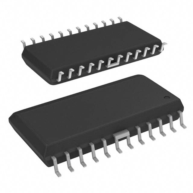
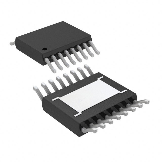
Allegro MicroSystems A8450KLB-T
- Part No.:
- A8450KLB-T
- Manufacturer:
- Allegro MicroSystems
- Category:
- Voltage Regulators - Linear + Switching
- Package:
- 24-SOIC (0.295", 7.50mm Width)
- Datasheet:
-
 A8450KLB-T.pdf
- Description:
- IC REG QUAD BUCK/LINEAR 24SOIC
- Quantity:
- Payment:

- Shipping:

Inventory:3,351
Please send an inquiry. Send us your inquiry, and we will respond immediately.
Product details
Overview
A8450KLB-T from Allegro MicroSystems is an automotive-grade multi-output power management IC integrating a 5.7 V buck converter, dual 5 V linear regulators (digital and analog), a fixed 3.3 V LDO, and an adjustable 1.2–3.3 V LDO - all operating from 6–45 V input and rated for –40°C to 135°C ambient. It delivers up to 200 mA per 5 V rail, supports ignition-switch enable via ENBAT, and provides thermal shutdown, short-to-battery protection on V5A, and < 0.5% V5A/V5D tracking for engine control units.
For engineers reviewing the A8450KLB-T datasheet, A8450KLB-T pinout, A8450KLB-T application, or A8450KLB-T equivalent, this page delivers verified electrical specs, validated SOIC-W-24 package mapping, confirmed fault/POR signaling behavior, and real-world automotive supply chain context - including thermal derating curves, foldback current limit thresholds, and external pass transistor interface requirements.
Technical Context
The A8450KLB-T implements a current-mode variable-frequency buck converter with soft-start, internal charge pump (CP1/CP2/VCP) for N-channel MOSFET gate drive, and 100% duty cycle capability below 12 V input. Its four regulated outputs are hierarchically dependent: VREG (5.7 V) powers all downstream LDOs, while V5A/V5D tracking is actively controlled across temperature.
Two independent enable inputs - high-voltage ENBAT (–0.3 to 45 V) and logic-level ENB (–0.3 to 6.5 V) - support ignition-synchronized wake-up and microcontroller-controlled reset. The integrated POR block uses external capacitor C9 to set adjustable delay (65–135 ms), and NFAULT signals thermal warning (160°C), V5A short-to-supply, or V5A/V5D undervoltage (4.36–4.75 V).
Key Specifications
| Parameter | Value and Actual Design Meaning |
|---|---|
| Input Voltage Range | 6–45 V - supports cold-crank (6 V) and load-dump (45 V) transients in 12 V/24 V automotive systems. |
| VREG Output | 5.50–5.80 V at 550 mA total load - primary supply for all internal LDOs; dropout mode active below 6.5 V VBB. |
| V5D / V5A Output | 4.9–5.1 V each, ±2% tolerance, 200 mA max - digitally isolated 5 V rail and short-to-battery-protected analog 5 V rail with < 0.5% tracking. |
| V33 Output | 3.234–3.366 V (±2%) - fixed 3.3 V LDO for MCU I/O or sensing, with 2.75–3.10 V UVLO threshold and 80 mV hysteresis. |
| VADJ Range | 1.2–3.3 V adjustable via FB pin (1.16–1.24 V reference) and external R1/R2 - enables core voltage scaling for DSPs or low-power MCUs. |
| Quiescent Current | <10 µA in disabled mode - meets automotive sleep-current requirements for always-on ECU modules. |
| Thermal Protection | Thermal warning at 160°C, shutdown at 175°C with 15°C hysteresis - prevents latch-up during under-hood thermal stress. |
Pinout & Package
Package: 24-pin SOIC-W surface-mount (suffix LB), with internally fused power ground pins (pins 6–7 and 18–19) yielding RθJA = 35°C/W on 4-layer PCB.
| Pin/Terminal | Circuit Role | Design Meaning |
|---|---|---|
| LX | Buck switch node | Connects to external inductor L1 and Schottky catch diode D1; swings between VBB and ~–2 V during switching. |
| ENBAT | High-voltage enable input | Accepts ignition/battery-switch signal (2.7–45 V); edge-triggered wake-up with <300 µA leakage at 45 V. |
| V33 | Fixed 3.3 V LDO output | Supplies MCU I/O or sensors; current-limited via CL33 pin and external R3 resistor (foldback to 40% of set limit). |
| V33BD | 3.3 V base drive output | Drives external npn pass transistor Q1 base; delivers 5–16 mA depending on VOUT and VREG headroom. |
| CL33 | 3.3 V current limit sense | Sets foldback threshold (175–225 mV) for V33 regulator; short to VREG disables current limiting. |
| GND | Power ground (pins 6, 7, 18, 19) | Internally fused for thermal robustness; multiple pins reduce impedance and improve heat spreading. |
| VREG | Buck converter output (5.7 V) | Primary supply for all LDOs; monitored for UVLO (4.94–5.36 V) and used to derive V5A/V5D/V33/VADJ. |
| V5D | Digital 5 V LDO output | 200 mA max, ±2% accuracy; undervoltage lockout at 4.24–4.75 V; no short-to-battery protection. |
| NFAULT | Open-drain fault indicator | Pulled low for V5A short-to-supply, TJ ≥160°C (warning), or V5A/V5D UVLO; sinks ≤1 µA when deasserted. |
| NPOR | Open-drain power-on-reset | Asserted low during V33/VADJ UVLO, VREG UVLO, or simultaneous ENBAT/ENB low; delay set by C9 on CPOR. |
| V5A | Analog 5 V LDO output | 200 mA max, ±2% accuracy, short-to-battery protected; tracks V5D within ±25 mV over full temperature range. |
| VBB | Main input supply | Accepts 6–45 V battery input; absolute max rating –40 V (reverse polarity tolerant only with external protection). |
| CP2 / CP1 / VCP | Charge pump terminals | CP1/CP2 connect to 0.1 µF ceramic (C8); VCP supplies boosted gate drive for internal N-MOSFET buck switch. |
| VREG11 | Internal reference bypass | Connect 0.1 µF ceramic capacitor to GND; stabilizes bandgap reference for VFB and UVLO comparators. |
| ENB | Logic-level enable input | Microcontroller-compatible (2.7–6.5 V); pulls device into reset when low; enables POR assertion on falling edge. |
| CPOR | POR delay capacitor connection | External capacitor C9 sets tPOR = 213 × C9 (µF → ms); 0.47 µF yields 100 ms typical delay. |
| CLADJ | Adjustable regulator current limit sense | Sets foldback threshold for VADJ output; same 175–225 mV range as CL33; short to VREG disables limiting. |
| VADJBD | Adjustable regulator base drive | Drives external npn pass transistor Q2 base; current scales with VREG–VADJ headroom for improved transient response. |
| FB | Feedback input for VADJ | 1.16–1.24 V reference; VADJ = VFB × (1 + R1/R2); bias current ±100 nA enables high-impedance resistor networks. |
| VIN | Internal VREG monitor | Not user-accessible; connects to internal VREG monitor for UVLO and POR generation. |
| H.V. | High-voltage protection node | Internal clamp for ENBAT overvoltage; not externally accessible - part of internal protection circuitry. |
| A8450 | Device identifier marker | Marking on package top surface; not an electrical pin - used for visual identification and traceability. |
Key Features
| Feature | Design Value |
|---|---|
| Dual 5 V tracking regulators | V5A and V5D maintain ≤±25 mV offset across –40°C to 135°C - eliminates need for external trimming in instrument clusters. |
| Short-to-battery protection on V5A | Active clamping prevents damage if V5A output contacts 12/24 V battery rail - critical for analog sensor front-ends. |
| Ignition-switch compatible enable | ENBAT accepts 2.7–45 V signals without level-shifting - directly interfaces with vehicle ignition switch or battery disconnect. |
| Adjustable 1.2–3.3 V LDO with base drive | VADJBD delivers up to 16 mA base current - enables use of cost-effective npn transistors (e.g., MPSW06) instead of integrated LDOs. |
| Thermal warning + shutdown | Separate 160°C warning (NFAULT) and 175°C shutdown with 15°C hysteresis - allows host MCU to initiate graceful shutdown before failure. |
| Configurable POR delay | tPOR set by single external capacitor (C9) - supports timing alignment with MCU boot sequence without firmware changes. |
Applications
| Engine Control Unit (ECU) | Advanced Driver Assistance Systems (ADAS) |
|---|---|
Use Scenario: Powers MCU core, CAN transceiver, and analog sensor interfaces in gasoline/diesel engine management modules exposed to under-hood temperatures up to 135°C. IC Role / Device Role / Timing Role: Central power hub delivering synchronized 5 V (digital/analog), 3.3 V, and adjustable core voltage - with ENBAT enabling crank detection and NPOR coordinating MCU reset timing. Use Value: Eliminates need for discrete DC-DC + multiple LDOs; < 0.5% V5A/V5D tracking ensures ADC reference stability; short-to-battery protection prevents field failures from wiring faults. |
Use Scenario: Supplies image signal processor (ISP), radar SoC, and camera sensor array in forward-facing ADAS cameras mounted behind windshield. IC Role / Device Role / Timing Role: Provides clean, tracked 5 V rails for analog front-end and digital logic, plus adjustable VADJ for ISP core voltage scaling - with thermal warning allowing predictive throttling. Use Value: Single-package solution reduces BOM count and PCB area; V5A short-to-battery protection safeguards camera analog outputs; 6–45 V input handles stop-start and load-dump events. |
| Body Control Module (BCM) | Infotainment Head Unit |
Use Scenario: Powers door module MCU, LIN transceivers, and LED drivers in centralized body electronics controlling lighting, locks, and windows. IC Role / Device Role / Timing Role: Delivers 3.3 V for MCU, dual 5 V for LIN and power switches, and adjustable VADJ for display backlight dimming - enabled via ENB from main BCM controller. Use Value: Foldback current limiting protects against shorted LED strings; <10 µA shutdown current meets OEM sleep-mode requirements; SOIC-W package supports automated optical inspection. |
Use Scenario: Supplies application processor, audio codec, and touch controller in automotive infotainment systems requiring multiple voltage domains and thermal resilience. IC Role / Device Role / Timing Role: Generates 5 V (analog for audio), 5 V (digital for processor I/O), 3.3 V (for memory), and 1.8 V (via VADJ) for DDR interface - coordinated by single POR signal. Use Value: Integrated tracking eliminates timing skew between audio and digital domains; thermal shutdown prevents thermal runaway during extended video playback; 45 V max input withstands jump-start conditions. |
Equivalent & Alternatives
The following parts are listed as comparable options for similar multi-rail automotive voltage regulator applications.
| Alternative Part | Technical Difference | Application Difference | Selection Advice |
|---|---|---|---|
| MAX25201ATPA/V+ (Maxim Integrated) | Single 5 V + 3.3 V outputs only; no adjustable VADJ or V5A short-to-battery protection; requires external tracking components. | Lacks V5A/V5D tracking and analog rail protection - unsuitable for safety-critical analog sensor supplies. | Choose for simpler 2-rail designs where VADJ and short-to-battery features are unnecessary. |
| TPS65381A-Q1 (Texas Instruments) | Three 5 V outputs (no 3.3 V), no adjustable regulator, higher quiescent current (25 µA), no ENBAT high-voltage enable. | Missing ignition-switch interface and fixed 3.3 V rail - cannot replace A8450KLB-T in ECU or BCM without redesign. | Prefer when system requires triple 5 V rails and has dedicated 3.3 V generation elsewhere. |
Compared with MAX25201ATPA/V+ and TPS65381A-Q1, the A8450KLB-T uniquely integrates V5A short-to-battery protection, ENBAT high-voltage enable, and factory-tracked V5A/V5D outputs - reducing external component count and enabling direct replacement in existing ECU layouts without layout changes.
Availability
A8450KLB-T is available at Aetrix Electronics and suitable for engine control units, ADAS camera modules, body control modules, and infotainment head units requiring stable component supply across automotive production lifecycles.
Supply support for A8450KLB-T includes scheduled delivery planning, volume procurement assistance, BOM continuity management, traceable sourcing, and lifecycle availability coordination for OEM customers, industrial embedded developers, connected-device designers, and electronics production programs.
Manufacturer
Allegro MicroSystems is a U.S.-based designer of high-performance power ICs and magnetic sensors for automotive and industrial markets, headquartered in Manchester, NH.
The A8450 product line targets automotive power management in extreme-temperature environments, specifically engineered to replace discrete buck + LDO solutions in ECUs, ADAS, and body electronics with integrated protection and tracking.
FAQ
What is the maximum load current supported by the A8450KLB-T's V5A and V5D outputs?
The A8450KLB-T delivers up to 200 mA per 5 V rail (V5A and V5D), with current limits of 200–300 mA typical. Both outputs feature foldback protection that reduces current to 50 mA during short-circuit events. The V5A rail adds short-to-battery protection, making it suitable for analog sensor interfaces where wiring faults could expose the output to battery voltage.
How does the A8450KLB-T achieve V5A/V5D output tracking, and what is its accuracy?
The A8450KLB-T achieves V5A/V5D tracking through an integrated analog control loop that actively adjusts V5A regulation to match V5D across temperature and load. Over the full –40°C to 135°C operating range and 50–200 mA load, tracking error is guaranteed within ±25 mV - equivalent to < 0.5% of nominal 5 V - eliminating need for external calibration in precision analog applications.
Can the A8450KLB-T operate during automotive cold-crank conditions?
Yes, the A8450KLB-T operates down to 6 V input and supports 100% duty cycle mode below 12 V, enabling continuous regulation during cold-crank (typically 6–8 V). Its VREG output remains functional down to 5.0 V in dropout mode, ensuring downstream LDOs stay powered. Input UVLO is absent - the device relies on external system-level protection for reverse polarity or extreme under-voltage.
What external components are required to configure the adjustable VADJ output of the A8450KLB-T?
To configure the A8450KLB-T's adjustable VADJ output (1.2–3.3 V), you must connect two external resistors (R1, R2) to the FB pin per VADJ = VFB × (1 + R1/R2), where VFB = 1.20 V typical. Additionally, a current-limiting resistor R4 connects to CLADJ to set foldback threshold (ICL = 200 mV / R4), and a base-drive capacitor (C4 ≥1 µF) stabilizes the external npn pass transistor Q2.
Does the A8450KLB-T require a heatsink in standard automotive applications?
No external heatsink is required for the A8450KLB-T in standard applications. Its SOIC-W-24 package achieves RθJA = 35°C/W on a 4-layer PCB, supporting up to 3.5 W dissipation at 125°C ambient. Derating curves confirm operation up to 135°C ambient at reduced power - sufficient for most ECU and BCM deployments without added thermal mass.
A8450KLB-T Specifications
- Product attributes
- Attribute value
- Manufacturer:
- Allegro MicroSystems
- Series:
- -
- Package/Case:
- 24-SOIC (0.295", 7.50mm Width)
- Packaging:
- Tube
- Product Status:
- Obsolete
- Topology:
- Step-Down (Buck) (1), Linear (LDO) (4)
- Number of Outputs:
- 4
- Frequency - Switching:
- -
- Voltage/Current - Output 1:
- 3.3V, 200mA
- Voltage/Current - Output 2:
- 1.2V ~ 3.3V, 200mA
- Voltage/Current - Output 3:
- 5V, 200mA
- w/LED Driver:
- No
- w/Supervisor:
- No
- w/Sequencer:
- Yes
- Voltage - Supply:
- 6V ~ 45V
- Operating Temperature:
- -40°C ~ 135°C
- Grade:
- -
- Qualification:
- -
- Mounting Type:
- Surface Mount
- Supplier Device Package:
- 24-SOIC
A8450KLB-T FAQ
1.How can I place an order for A8450KLB-T through Aetrix?
Please submit a Request for Quotation (RFQ) for A8450KLB-T on Aetrix. Our sales agent will provide a competitive quotation and guide you through the order confirmation once you accept the terms.
2.Are the price and stock information for A8450KLB-T reliable?
The price and inventory of A8450KLB-T are updated periodically and may fluctuate due to market conditions. Stock and pricing data are typically refreshed every 24 hours. Quotation validity for A8450KLB-T is usually 5 days.
3.What payment methods are accepted for A8450KLB-T?
We accept Wire Transfer, PayPal, Credit Card, Western Union, MoneyGram, and Escrow for A8450KLB-T transactions.
Note: Certain payment methods may incur a processing fee.
4.How is shipping managed for A8450KLB-T?
A8450KLB-T orders can be shipped via leading logistics carriers, including DHL, UPS, FedEx, TNT, or Registered Mail.
Once your A8450KLB-T order is processed, you will receive an email with the shipment details and tracking number.
Note: Tracking information may take up to 24 hours to appear. Express delivery typically takes 3–5 business days.
5.How can I obtain technical support or documentation for A8450KLB-T?
For technical support, including A8450KLB-T datasheets, pinout diagrams, or application guidance, please contact our engineering support team. They can provide detailed documentation and assistance for your A8450KLB-T requirements.
6.How does Aetrix verify that A8450KLB-T is sourced from the original manufacturer or authorized distributors?
All A8450KLB-T products on Aetrix are procured from qualified distributors and authorized channels. Our dedicated quality assurance team conducts strict verification, including traceability checks and, if necessary, third-party testing. This ensures that A8450KLB-T meets industry standards.
7.What is the process for return or replacement of A8450KLB-T?
All A8450KLB-T units undergo pre-shipment inspection (PSI). If there is an issue with A8450KLB-T, returns or replacements are accepted under the following conditions:
1.Quantity discrepancies, incorrect items, or visible external defects (such as breakage or corrosion), acknowledged by Aetrix.
2.The issue is reported within 90 days of delivery.
3.The A8450KLB-T part is unused and in its original packaging.
Return procedure for A8450KLB-T:
1.Submit a request within 90 days.
2.Obtain a Return Material Authorization (RMA) from Aetrix.
A8450KLB-T Tags

-
TPS6521905RHBR
Texas Instruments
-
MIC3385YHL-TR
Microchip Technology
-
A4402ELPTR-T
Allegro MicroSystems

-
LM26480SQ-AA/NOPB
Texas Instruments
-
A4402KLPTR-T
Allegro MicroSystems
-
BD71847AMWV-E2
ROHM Semiconductor
-
ADP5040ACPZ-1-R7
Analog Devices Inc.
-
LT3048IDC#TRPBF
Analog Devices Inc.
-
ADP5037ACPZ-R7
Analog Devices Inc.

-
XRP7714ILB-F
MaxLinear, Inc.
-
LTC3260EDE#TRPBF
Analog Devices Inc.
-
LTC3260EMSE#PBF
Analog Devices Inc.
Tech Hub

A practical engineering and sourcing framework covering lifecycle verification, lifetime-buy calculations, replacement qualification, supplier checks and counterfeit-risk controls.

TTL and CMOS logic families differ in thresholds, loading, output drive, power and timing. This engineering guide compares 74HC and 74HCT, calculates noise margins and checks 3.3 V/5 V compatibility.

A practical engineering guide to 3.3V and 5V logic compatibility, input thresholds, resistor dividers, translator ICs, MOSFET level shifting, I2C pull-ups, timing limits and power-sequencing risks.

The 74HC595 uses push-pull logic outputs, while the TPIC6B595 uses 50 V open-drain DMOS sinks for higher-power loads. This guide compares timing, current limits, 3.3 V interfacing, load wiring, thermal…

The 74HC595 converts serial data into eight stable parallel outputs. This guide covers pin functions, shift and storage timing, OE and MR behavior, drive-current limits, cascading, voltage compatibilit…

A technical comparison of level-sensitive latches and edge-triggered flip-flops, covering timing windows, setup and hold limits, master–slave operation, time borrowing, race-through, HDL inference and…

A D latch stores one bit while Enable controls when data can pass. This reference covers gate-level operation, truth tables, transparency, setup and hold timing, LE versus OE, common ICs and practical …

An SR latch stores one bit through cross-coupled feedback. This engineering reference covers NOR and NAND implementations, truth tables, forbidden-state recovery, gated operation, switch debouncing, fa…

Latch circuits retain one bit through feedback. This technical reference covers SR and D latches, truth tables, transparency, timing limits, latch-versus-flip-flop behavior, applications and common log…

An engineering guide to LED driver operation, constant-current and constant-voltage outputs, linear and switching topologies, dimming, IC selection, calculations, replacement compatibility, and fault c…


