
 My Inquiry
 My Account


Allegro MicroSystems A8904SLB
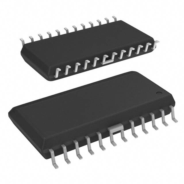
- Part No.:
- A8904SLB
- Manufacturer:
- Allegro MicroSystems
- Category:
- Motor Drivers, Controllers
- Package:
- 24-SOIC (0.295", 7.50mm Width)
- Datasheet:
-
 A8904SLB.pdf
- Description:
- IC MOTOR DRIVER 4.5V-5.5V 24SOIC
- Quantity:
- Payment:

- Shipping:

Inventory:2,717
Please send an inquiry. Send us your inquiry, and we will respond immediately.
Product details
Overview
A8904SLB from Allegro MicroSystems is a 3-phase brushless DC motor controller/driver with integrated back-EMF sensing, sensorless commutation, and programmable digital frequency-locked loop (FLL) speed control. It delivers up to 1.2 A per phase via low-RDS(on) N-channel DMOS half-bridges, supports external tachometer input on SECTOR DATA, and operates with VBB up to 14 V and VDD = 5 V. It is used in high-speed spindle control for optical drives and precision cooling fans.
For engineers reviewing the A8904SLB datasheet, A8904SLB pinout, A8904SLB application, or A8904SLB equivalent, key selection considerations include its 24-pin SOICW (LB) package with fused thermal leads, programmable transconductance gain (250/500 mA/V), serial port configuration of start-up current limit and direction, and FLL-based closed-loop speed regulation without Hall sensors.
Technical Context
The A8904SLB implements adaptive commutation using back-EMF zero-crossing detection at the high-impedance output terminal, synchronized by FCOM toggling and controlled by CD1/CD2 timing capacitors. Its linear current-mode control uses FILTER terminal voltage to drive low-side MOSFETs via transconductance stage with internal sense resistor RS (200 mΩ).
Start-up is managed by a dedicated CST oscillator and watchdog circuitry (CWD capacitor), while dynamic braking is enabled either externally via BRAKE pin or through serial port command. The device integrates charge pump for high-side gate drive, intrinsic clamp diodes, and full protection including programmable overcurrent limit, thermal shutdown (165°C), and logic undervoltage lockout (3.6–3.9 V).
Key Specifications
| Parameter | Value and Actual Design Meaning |
|---|---|
| VBB Range | 4.0–14 V: Supports 5 V or 12 V motor supplies; limits maximum winding voltage and power stage headroom. |
| Max Output Current | 1.2 A continuous (D3=0,D4=0,D28=0): Configurable down to 125 mA via serial port bits for torque/speed trade-off. |
| Transconductance Gain | 500 mA/V (D28=0) or 250 mA/V (D28=1): Sets current-to-voltage conversion ratio for linear motor current control. |
| FLL Oscillator Frequency | Up to 20 MHz: Determines resolution and response speed of internal speed reference counter (REF). |
| Serial Port Clock Max | 3.3 MHz: Enables fast configuration of 29-bit register including poles, direction, sleep mode, and diagnostics. |
| Thermal Shutdown | 165°C with 20°C hysteresis: Protects die during overload; triggers HIGH on DATA OUT for system-level fault reporting. |
| rDS(on) Total | 1.0 Ω typical (source + sink + RS): Defines conduction loss and thermal dissipation in half-bridge power stage. |
Pinout & Package
Package: 24-pin wide-body SOIC (LB), lead-free with 100% matte tin plating, 4 internally fused leads for enhanced thermal dissipation, overall height <1.2 mm.
| Pin/Terminal | Circuit Role | Design Meaning |
|---|---|---|
| 1 (VBB) | Load supply input | Primary motor power rail; connects to 5–14 V source and bulk decoupling capacitor. |
| 5 (OUTA), 8 (OUTB), 9 (OUTC) | Half-bridge outputs | Drive motor phases A/B/C; each capable of 1.2 A sink/source with integrated DMOS and clamp diodes. |
| 6–7, 18–19 (GROUND) | Power and logic ground | Common return path for motor current, logic, and thermal heat sink; must be low-impedance PCB plane. |
| 10 (CENTERTAP) | Back-EMF reference node | Connects to motor star point; used as comparator reference for zero-crossing detection during commutation. |
| 11 (BRAKE) | Active-low dynamic brake control | Pulls all three outputs low simultaneously; external RC sets brake delay; also controllable via serial port. |
| 13 (FILTER) | Speed error integrator node | Voltage here sets motor current via transconductance stage; external RC defines loop stability and response. |
| 14 (SECTOR DATA) | External tachometer input | Accepts sector/index pulses for high-precision speed feedback; enables hybrid internal/external FLL operation. |
| 15 (VDD) | Logic supply input | 5 V ±5% digital supply; UVLO activates below 3.6 V to prevent erratic register behavior. |
| 17 (DATA OUT) | Multiplexed diagnostic output | Outputs TACH, FCOM, SYNC, or thermal shutdown status based on D22/D23 serial bits. |
| 20 (RESET) | Active-low sleep mode entry | Pulling low clears serial register and forces chip into low-power sleep (250–500 μA IDD). |
| 21 (CHIP SELECT), 22 (CLOCK), 23 (DATA IN) | Serial interface control | 3-wire SPI-compatible port for programming 29-bit register; min. CS high time = 500 ns. |
| 24 (CD1), 2 (CD2), 3 (CWD), 4 (CST), 12 (CRES) | Timing and reservoir capacitors | Set commutation delay (CD1/CD2), blanking/watchdog (CWD), start-up oscillator (CST), and gate drive charge (CRES). |
Key Features
| Feature | Design Value |
|---|---|
| Sensorless commutation with adaptive delay | Uses CD1/CD2 discharge timing triggered by FCOM to advance state sequencer at optimal electrical angle, compensating for winding inductance. |
| Programmable transconductance gain | 250 mA/V or 500 mA/V selectable via D28: allows matching of current loop gain to motor Kt and system inertia. |
| YANK speed loop initialization | Pulls FILTER to VFILTERTH at startup to force max current until first ERROR FAST signal, ensuring reliable spin-up under load. |
| Real-time diagnostic multiplexing | DATA OUT outputs TACH, FCOM, SYNC, or thermal shutdown status-enables live debugging without additional test points. |
| Configurable overcurrent protection | Eight current limit settings (125–1400 mA) via D3/D4/D28: permits staged limiting during start-up vs. run conditions. |
Applications
| Optical Disk Drive Spindle Control | High-Speed Cooling Fan Regulation |
|---|---|
|
Use Scenario: Precise constant-speed rotation of Blu-ray or DVD spindle motors under variable mechanical load and temperature. IC Role / Device Role / Timing Role: Primary motor controller executing sensorless commutation, FLL-based speed regulation, and real-time thermal monitoring. Use Value: Eliminates Hall sensors and reduces BOM cost while maintaining <±0.5% speed accuracy across 5,000–20,000 rpm range. |
Use Scenario: Quiet, responsive airflow control in server chassis and telecom equipment with rapid thermal transient response. IC Role / Device Role / Timing Role: Closed-loop BLDC driver using external tachometer pulses (SECTOR DATA) for jitter-free speed tracking. Use Value: Achieves <2% speed deviation during step-load changes via programmable FILTER loop compensation and 3.3 MHz serial reconfiguration. |
| Industrial Pump Motor Control | Medical Centrifuge Drive |
|
Use Scenario: Reliable start-up and stall recovery in 24 V brushless pumps handling viscous fluids with high inertia. IC Role / Device Role / Timing Role: Integrates watchdog-triggered commutation, dynamic braking (BRAKE pin), and programmable start-up current limit. Use Value: Guarantees restart after stall via CWD-based timeout and automatic direction correction without microcontroller intervention. |
Use Scenario: Safe, repeatable acceleration/deceleration profiles in Class II medical centrifuges requiring precise rotor balance and fault logging. IC Role / Device Role / Timing Role: Safety-critical motor controller providing thermal shutdown indication (DATA OUT), sleep mode for standby, and real-time FCOM monitoring. Use Value: Enables FDA-compliant event logging via serial port readback of diagnostic flags and thermal history without external ADC. |
Equivalent & Alternatives
The following parts are listed as comparable options for similar 3-phase BLDC controller applications.
| Alternative Part | Technical Difference | Application Difference | Selection Advice |
|---|---|---|---|
| A8902CLBA | Pin-for-pin compatible but lacks serial port programmability; fixed transconductance (500 mA/V) and no external tachometer input. | Used in cost-sensitive, static-configured optical drives where field updates or diagnostics are unnecessary. | Select A8904SLB when serial reconfiguration, dual-gain support, or SECTOR DATA integration is required. |
| DRV10983ZRGTT | TI device with integrated MOSFETs (3 A), no external CD/CWD timing caps, and I²C interface instead of SPI-like serial port. | Targets compact fan modules with minimal external components; lacks centertap-based back-EMF sensing architecture. | Choose A8904SLB for designs requiring discrete power stage flexibility, centertap sensing, or legacy A8902 migration path. |
Compared with A8902CLBA and DRV10983ZRGTT, the A8904SLB uniquely combines programmable sensorless commutation timing, dual transconductance gain, and real-time diagnostic multiplexing in a thermally optimized SOICW package-making it optimal for upgrade paths and applications demanding configurability without sacrificing robustness.
Availability
A8904SLB is available at Aetrix Electronics and suitable for optical drive spindle control, high-speed cooling fan regulation, and industrial pump motor control requiring stable component supply, long-term lifecycle assurance, and traceable sourcing.
Supply support for A8904SLB includes scheduled delivery planning, volume procurement assistance, BOM continuity management, traceable sourcing, and lifecycle availability coordination for OEM customers, industrial embedded developers, connected-device designers, and electronics production programs.
Manufacturer
Allegro MicroSystems is a U.S.-based designer of high-performance magnetic sensing and power IC solutions, founded in 1989 and headquartered in Worcester, Massachusetts.
The A8904 belongs to Allegro's family of integrated BLDC motor controllers fabricated in BCD process, engineered specifically for sensorless, high-efficiency spindle and fan control in consumer and industrial systems.
FAQ
What is the package type and thermal performance of the A8904SLB?
The A8904SLB uses a 24-pin wide-body SOIC (LB) package with four internally fused leads for enhanced thermal dissipation. Its junction-to-ambient thermal resistance is 35°C/W on a 4-layer JEDEC-standard PCB, enabling reliable 1.2 A continuous operation at 85°C ambient without external heatsinking. The package is lead-free with 100% matte tin plating.
How does the A8904SLB achieve sensorless commutation without Hall effect sensors?
The A8904SLB detects back-EMF zero crossings at the high-impedance motor phase relative to the CENTERTAP voltage, generating FCOM toggles. Adaptive commutation delay is implemented using CD1/CD2 capacitor discharge timing triggered by FCOM edges, advancing the six-state sequencer at optimal electrical angles-even under varying load and speed conditions.
Can the A8904SLB be used with an external tachometer signal instead of internal back-EMF sensing?
Yes-the A8904SLB supports external speed feedback via the SECTOR DATA pin. When D19 = 1 is programmed via serial port, the device accepts sector or index pulses to generate the TACH signal, enabling hybrid or fully external speed control while retaining internal FLL loop integrity and diagnostic capabilities.
What protection features are built into the A8904SLB?
The A8904SLB integrates programmable overcurrent limiting (eight settings via D3/D4/D28), thermal shutdown at 165°C with 20°C hysteresis, logic undervoltage lockout (3.6–3.9 V), and intrinsic clamp diodes across all outputs. Fault status is reported in real time on DATA OUT, and dynamic braking is supported via BRAKE pin or serial command.
Is the A8904SLB pin-compatible with earlier Allegro motor drivers?
Yes-the A8904SLB is specified as a pin-for-pin replacement for the A8902CLBA. All critical pins (VBB, OUTA/B/C, CENTERTAP, BRAKE, FILTER, SECTOR DATA, etc.) retain identical placement and function. However, the A8904SLB adds serial port pins (CHIP SELECT, CLOCK, DATA IN, DATA OUT) and expands functionality beyond the A8902CLBA's fixed configuration.
A8904SLB Specifications
- Product attributes
- Attribute value
- Manufacturer:
- Allegro MicroSystems
- Series:
- -
- Package/Case:
- 24-SOIC (0.295", 7.50mm Width)
- Packaging:
- Tube
- Product Status:
- Obsolete
- Motor Type - Stepper:
- -
- Motor Type - AC, DC:
- Brushless DC (BLDC)
- Function:
- Controller - Commutation, Direction Management
- Output Configuration:
- Pre-Driver - Half Bridge (3)
- Interface:
- SPI
- Technology:
- CMOS, DMOS
- Step Resolution:
- -
- Applications:
- General Purpose
- Current - Output:
- -
- Voltage - Supply:
- 4.5V ~ 5.5V
- Voltage - Load:
- 4V ~ 14V
- Operating Temperature:
- -20°C ~ 85°C (TA)
- Grade:
- -
- Qualification:
- -
- Mounting Type:
- Surface Mount
- Supplier Device Package:
- 24-SOIC
A8904SLB FAQ
1.How can I place an order for A8904SLB through Aetrix?
Please submit a Request for Quotation (RFQ) for A8904SLB on Aetrix. Our sales agent will provide a competitive quotation and guide you through the order confirmation once you accept the terms.
2.Are the price and stock information for A8904SLB reliable?
The price and inventory of A8904SLB are updated periodically and may fluctuate due to market conditions. Stock and pricing data are typically refreshed every 24 hours. Quotation validity for A8904SLB is usually 5 days.
3.What payment methods are accepted for A8904SLB?
We accept Wire Transfer, PayPal, Credit Card, Western Union, MoneyGram, and Escrow for A8904SLB transactions.
Note: Certain payment methods may incur a processing fee.
4.How is shipping managed for A8904SLB?
A8904SLB orders can be shipped via leading logistics carriers, including DHL, UPS, FedEx, TNT, or Registered Mail.
Once your A8904SLB order is processed, you will receive an email with the shipment details and tracking number.
Note: Tracking information may take up to 24 hours to appear. Express delivery typically takes 3–5 business days.
5.How can I obtain technical support or documentation for A8904SLB?
For technical support, including A8904SLB datasheets, pinout diagrams, or application guidance, please contact our engineering support team. They can provide detailed documentation and assistance for your A8904SLB requirements.
6.How does Aetrix verify that A8904SLB is sourced from the original manufacturer or authorized distributors?
All A8904SLB products on Aetrix are procured from qualified distributors and authorized channels. Our dedicated quality assurance team conducts strict verification, including traceability checks and, if necessary, third-party testing. This ensures that A8904SLB meets industry standards.
7.What is the process for return or replacement of A8904SLB?
All A8904SLB units undergo pre-shipment inspection (PSI). If there is an issue with A8904SLB, returns or replacements are accepted under the following conditions:
1.Quantity discrepancies, incorrect items, or visible external defects (such as breakage or corrosion), acknowledged by Aetrix.
2.The issue is reported within 90 days of delivery.
3.The A8904SLB part is unused and in its original packaging.
Return procedure for A8904SLB:
1.Submit a request within 90 days.
2.Obtain a Return Material Authorization (RMA) from Aetrix.
A8904SLB Tags

-
DRV2603RUNR
Texas Instruments

-
DRV8837CDSGR
Texas Instruments

-
DRV8837DSGR
Texas Instruments
-
DRV8838DSGR
Texas Instruments

-
DRV8839DSSR
Texas Instruments

-
EMC2301-1-ACZL-TR
Microchip Technology
-
DRV8231ADSGR
Texas Instruments

-
EMC2302-2-AIZL-TR
Microchip Technology

-
DRV8800PWPR
Texas Instruments
-
DRV8835DSSR
Texas Instruments

-
EMC2303-1-KP-TR
Microchip Technology

-
DRV8876PWPR
Texas Instruments
Tech Hub

A practical engineering and sourcing framework covering lifecycle verification, lifetime-buy calculations, replacement qualification, supplier checks and counterfeit-risk controls.

TTL and CMOS logic families differ in thresholds, loading, output drive, power and timing. This engineering guide compares 74HC and 74HCT, calculates noise margins and checks 3.3 V/5 V compatibility.

A practical engineering guide to 3.3V and 5V logic compatibility, input thresholds, resistor dividers, translator ICs, MOSFET level shifting, I2C pull-ups, timing limits and power-sequencing risks.

The 74HC595 uses push-pull logic outputs, while the TPIC6B595 uses 50 V open-drain DMOS sinks for higher-power loads. This guide compares timing, current limits, 3.3 V interfacing, load wiring, thermal…

The 74HC595 converts serial data into eight stable parallel outputs. This guide covers pin functions, shift and storage timing, OE and MR behavior, drive-current limits, cascading, voltage compatibilit…

A technical comparison of level-sensitive latches and edge-triggered flip-flops, covering timing windows, setup and hold limits, master–slave operation, time borrowing, race-through, HDL inference and…

A D latch stores one bit while Enable controls when data can pass. This reference covers gate-level operation, truth tables, transparency, setup and hold timing, LE versus OE, common ICs and practical …

An SR latch stores one bit through cross-coupled feedback. This engineering reference covers NOR and NAND implementations, truth tables, forbidden-state recovery, gated operation, switch debouncing, fa…

Latch circuits retain one bit through feedback. This technical reference covers SR and D latches, truth tables, transparency, timing limits, latch-versus-flip-flop behavior, applications and common log…

An engineering guide to LED driver operation, constant-current and constant-voltage outputs, linear and switching topologies, dimming, IC selection, calculations, replacement compatibility, and fault c…


