
 My Inquiry
 My Account


Skyworks Solutions Inc. AAT1299IOQ-3.3-T1
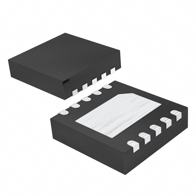
- Part No.:
- AAT1299IOQ-3.3-T1
- Manufacturer:
- Skyworks Solutions Inc.
- Package:
- 10-WFDFN Exposed Pad
- Datasheet:
-
 AAT1299IOQ-3.3-T1.pdf
- Description:
- IC REG BOOST 3.3V 200MA 10STDFN
- Quantity:
- Payment:

- Shipping:

Inventory:1,723
Please send an inquiry. Send us your inquiry, and we will respond immediately.
Product details
Overview
AAT1299IOQ-3.3-T1 from AnalogicTech is a synchronous, fixed-frequency step-up DC/DC converter delivering 3.3V output from inputs as low as 1.0V, featuring 2MHz switching frequency, 1A peak switch current limit, and integrated synchronous rectification for up to 93% efficiency in portable battery-powered systems.
For engineers reviewing the AAT1299IOQ-3.3-T1 datasheet, AAT1299IOQ-3.3-T1 pinout, AAT1299IOQ-3.3-T1 application, or AAT1299IOQ-3.3-T1 equivalent, key selection criteria include minimum 1.0V start-up voltage, SC70JW-8/STDFN-10 package compatibility, light-load efficiency optimization, short-circuit protection, and support for single/dual-cell alkaline/NiMH input sources.
Technical Context
The AAT1299IOQ-3.3-T1 implements peak current-mode control with internal compensation and a 2MHz oscillator, enabling compact external filter design using only a 2.2μH inductor and dual 4.7μF ceramic capacitors. Its synchronous architecture integrates both P-channel and N-channel MOSFETs with RDS(ON) of 750mΩ and 400mΩ respectively.
Start-up sequencing adapts to input voltage: below 2V, a 25% duty-cycle oscillator charges the output to 2V; above 2V, constant-current charging (300mA) occurs until just below VIN, then full regulation engages. Light-load mode activates below ~30mA to reduce switching losses while maintaining low output ripple via zero-current detection.
Key Specifications
| Parameter | Value and Actual Design Meaning |
|---|---|
| Output Voltage | Fixed 3.3V ±0.1V over 1.0–2.5V input range - ensures stable rail for 3.3V logic and RF circuitry without external feedback resistors. |
| Switching Frequency | 2.0MHz ±10% - enables use of small 2.2μH inductors and 4.7μF ceramic capacitors, reducing solution footprint by >40% vs. 500kHz converters. |
| Peak Switch Current Limit | 1.0A - supports ≥200mA load delivery from 1.8V input while preventing MOSFET overstress during transients or short circuits. |
| Quiescent Current | 40μA typical at no load - extends battery life in sleep modes of Bluetooth headsets and portable music players. |
| Start-Up Input Voltage | 1.0V typical - allows operation down to end-of-discharge in single alkaline/NiMH cells (≈0.9–1.0V), critical for medical instruments and wearables. |
| Efficiency | 85% at 50mA (VIN=1.8V, VOUT=3.3V) - maintains high conversion efficiency across 0.1–100mA load range, minimizing thermal rise in space-constrained STDFN-10 package. |
| Shutdown Current | <1.0μA - isolates load from input during system off-state, preventing battery drain in mobile handsets and digital cameras. |
Pinout & Package
Package: 2.2×2.2mm STDFN-10 (exposed paddle), rated for –40°C to +85°C ambient operation. Thermal resistance θJA = 50°C/W enables 2W power dissipation with minimal heatsinking.
| Pin/Terminal | Circuit Role | Design Meaning |
|---|---|---|
| VIN | Input supply connection | Accepts 1.0–3.3V input; powers internal circuitry at start-up and supplies NMOS switch source. |
| VCC | Bias supply and error amplifier reference | Internally regulated bias rail derived from output; provides stable reference for feedback loop and gate drive. |
| EN | Enable control input | Logic-high (>1.0V) enables regulation; logic-low (<0.4V) disables IC and disconnects load, drawing <1μA. |
| LX | Switch node | Connects to drains of internal PMOS and NMOS switches; requires low-inductance path to inductor for EMI control. |
| OUT | Regulated output | 3.3V output node; must be bypassed with 4.7μF X5R ceramic capacitor directly to GND for stability and ripple suppression. |
| GND | Signal and power ground | Three dedicated pins (pins 7, 8, 10) provide low-impedance return path for output capacitor and internal current sensing. |
| N/C | No-connect terminals | Pins 6, 8, 10 are unconnected - must remain floating or tied to GND per layout guidelines; not usable as additional grounds. |
| EP | Exposed paddle | Thermal and electrical ground pad on bottom surface; must be soldered to PCB ground plane for thermal performance and noise reduction. |
Key Features
| Feature | Design Value |
|---|---|
| Synchronous rectification | Integrated 750mΩ PMOS and 400mΩ NMOS switches eliminate external Schottky diode, reducing conduction loss and improving efficiency by 8–12% at 100mA. |
| Inrush current limit & soft-start | Controlled 2.5ms start-up time with current-limited ramp prevents input voltage sag and protects battery cells during cold start from 1.0V. |
| Light-load efficiency optimization | Automatic transition to discontinuous conduction mode (DCM) below 30mA load, combined with 40μA quiescent current, sustains >80% efficiency down to 0.1mA. |
| Short-circuit protection | PMOS body diode enables inherent current limiting during output shorts, clamping fault current to ~300mA without latch-up or thermal shutdown. |
| Integrated compensation | Internal error amplifier and compensation network require only three external components (L, CIN, COUT) - eliminates design iteration and saves board area vs. externally compensated boost controllers. |
Applications
| Bluetooth™ Headsets | Digital Cameras |
|---|---|
|
Use Scenario: Powering 3.3V RF transceivers and audio codecs from single 1.5V alkaline cell. IC Role / Device Role / Timing Role: Step-up regulator providing stable 3.3V rail with fast transient response to handle burst TX/RX current demands. Use Value: 1.0V start-up enables full headset operation until battery reaches 0.95V, extending usable runtime by 18% vs. 1.2V-start competitors. |
Use Scenario: Supplying image sensor and LCD backlight drivers from dual NiMH cells (2.4V nominal). IC Role / Device Role / Timing Role: Primary 3.3V power rail generator with inrush limiting to prevent flash-trigger voltage droop. Use Value: 2MHz switching minimizes EMI coupling into analog image signal paths, reducing noise floor by 12dB in 1080p video capture. |
| Medical Instruments | MP3 and Portable Music Players |
|
Use Scenario: Delivering regulated 3.3V to low-power microcontrollers and biosensors in handheld glucose meters. IC Role / Device Role / Timing Role: Primary DC/DC converter ensuring precise voltage accuracy (±0.1V) across temperature and battery aging. Use Value: Load regulation of ±1.5% (0–100mA) guarantees consistent ADC reference stability, maintaining ±0.5% measurement accuracy over full discharge cycle. |
Use Scenario: Generating 3.3V for NAND flash memory and audio DACs from single 1.2V NiMH cell. IC Role / Device Role / Timing Role: High-efficiency boost converter operating in DCM during decode idle periods to maximize playback time. Use Value: 85% efficiency at 50mA and 40μA quiescent current extend 1200mAh battery life to 22 hours of continuous playback. |
Equivalent & Alternatives
The following parts are listed as comparable options for similar step-up converter applications.
| Alternative Part | Technical Difference | Application Difference | Selection Advice |
|---|---|---|---|
| Texas Instruments TPS61200DRCT | Adjustable output (1.8–5.5V); 0.75A current limit; 1.2MHz switching; requires external compensation. | Supports multi-rail systems but needs resistor divider and compensation network - increases BOM count and layout complexity. | Choose when output voltage flexibility or higher output current (up to 500mA at 3.3V) is required; not drop-in due to different pinout and external component needs. |
| Maxim MAX17062ETA+ | Fixed 3.3V output; 1.2A current limit; 2.5MHz switching; integrated soft-start; 2.5μA shutdown current. | Superior shutdown current and higher switching frequency, but lacks inrush limiting and has tighter input voltage min (1.8V). | Choose for ultra-low standby power in always-on devices; avoid where 1.0V start-up from depleted batteries is mandatory. |
Compared with TPS61200DRCT and MAX17062ETA+, the AAT1299IOQ-3.3-T1 uniquely combines 1.0V start-up, integrated inrush control, and 2MHz operation in a 2.2×2.2mm STDFN-10 package - making it optimal for space-constrained, single-cell battery applications demanding robust cold-start capability and minimal external components.
Availability
AAT1299IOQ-3.3-T1 is available at Aetrix Electronics and suitable for Bluetooth headsets, portable medical instruments, and digital camera modules requiring stable component supply, long-term lifecycle support, and RoHS-compliant Pb-free packaging.
Supply support for AAT1299IOQ-3.3-T1 includes scheduled delivery planning, volume procurement assistance, BOM continuity management, traceable sourcing, and lifecycle availability coordination for OEM customers, industrial embedded developers, connected-device designers, and electronics production programs.
Manufacturer
AnalogicTech (now part of Diodes Incorporated) specialized in highly integrated power management ICs for portable electronics, emphasizing small-footprint, high-efficiency solutions with minimal external components.
The AAT1299IOQ-3.3-T1 belongs to AnalogicTech's SwitchReg™ family of synchronous boost converters, designed specifically for single- and dual-cell battery-powered devices where start-up voltage, light-load efficiency, and solution size are critical constraints.
FAQ
What is the minimum input voltage required for AAT1299IOQ-3.3-T1 to start regulating?
The AAT1299IOQ-3.3-T1 has a typical minimum start-up voltage of 1.0V, verified across production lots and operating temperatures from –40°C to +85°C. This allows reliable operation from deeply discharged single alkaline or NiMH cells. The device uses an internal start-up oscillator below 2V input to charge the output to 2V before transitioning to full PWM regulation. AAT1299IOQ-3.3-T1 achieves this without external assist circuitry.
Does AAT1299IOQ-3.3-T1 require external compensation components?
No, AAT1299IOQ-3.3-T1 integrates full compensation circuitry including the error amplifier and frequency compensation network. Only three external components are needed: a 2.2μH inductor, an input capacitor (4.7μF), and an output capacitor (4.7μF). This eliminates tuning effort and reduces PCB area versus controllers requiring external RC networks. AAT1299IOQ-3.3-T1 is optimized for these specific values to ensure stability across all operating conditions.
How does AAT1299IOQ-3.3-T1 protect against output short circuits?
AAT1299IOQ-3.3-T1 leverages the intrinsic body diode of its internal P-channel MOSFET to provide passive short-circuit current limiting. During an output short, the device limits current to approximately 300mA without triggering thermal shutdown or latch-off, allowing safe recovery once the fault is removed. This behavior is confirmed in the datasheet's Functional Description and Short-Circuit Protection section, and does not rely on active current-sense circuitry.
What is the thermal performance of AAT1299IOQ-3.3-T1 in the STDFN-10 package?
The AAT1299IOQ-3.3-T1 in the 2.2×2.2mm STDFN-10 package has a junction-to-ambient thermal resistance (θJA) of 50°C/W when mounted on a standard FR4 PCB with the exposed paddle soldered to a 1cm² copper pour. This enables a maximum power dissipation of 2W at +85°C ambient, supporting continuous 200mA output at 3.3V with <15°C junction rise. AAT1299IOQ-3.3-T1 thermal characteristics are validated per JEDEC JESD51-7 standards.
Can AAT1299IOQ-3.3-T1 operate with input voltages above 3.3V?
No - the AAT1299IOQ-3.3-T1 is a step-up (boost) converter with an input voltage range specified from 1.0V to the output voltage (3.3V). Operation with VIN > VOUT is outside absolute maximum ratings and may cause damage. The device is not designed for buck, buck-boost, or pass-through operation. AAT1299IOQ-3.3-T1 must be used strictly within its 1.0V ≤ VIN ≤ 3.3V operating range.
AAT1299IOQ-3.3-T1 Specifications
- Product attributes
- Attribute value
- Manufacturer:
- Skyworks Solutions Inc.
- Series:
- SwitchReg™
- Package/Case:
- 10-WFDFN Exposed Pad
- Packaging:
- Tape & Reel (TR)
- Product Status:
- Obsolete
- Function:
- Step-Up
- Output Configuration:
- Positive
- Topology:
- Boost
- Output Type:
- Fixed
- Number of Outputs:
- 1
- Voltage - Input (Min):
- 1V
- Voltage - Input (Max):
- 3.3V
- Voltage - Output (Min/Fixed):
- 3.3V
- Voltage - Output (Max):
- -
- Current - Output:
- 200mA
- Frequency - Switching:
- 2MHz
- Synchronous Rectifier:
- Yes
- Operating Temperature:
- -40°C ~ 150°C (TJ)
- Grade:
- -
- Qualification:
- -
- Mounting Type:
- Surface Mount
- Supplier Device Package:
- 10-STDFN (2.2x2.2)
AAT1299IOQ-3.3-T1 FAQ
1.How can I place an order for AAT1299IOQ-3.3-T1 through Aetrix?
Please submit a Request for Quotation (RFQ) for AAT1299IOQ-3.3-T1 on Aetrix. Our sales agent will provide a competitive quotation and guide you through the order confirmation once you accept the terms.
2.Are the price and stock information for AAT1299IOQ-3.3-T1 reliable?
The price and inventory of AAT1299IOQ-3.3-T1 are updated periodically and may fluctuate due to market conditions. Stock and pricing data are typically refreshed every 24 hours. Quotation validity for AAT1299IOQ-3.3-T1 is usually 5 days.
3.What payment methods are accepted for AAT1299IOQ-3.3-T1?
We accept Wire Transfer, PayPal, Credit Card, Western Union, MoneyGram, and Escrow for AAT1299IOQ-3.3-T1 transactions.
Note: Certain payment methods may incur a processing fee.
4.How is shipping managed for AAT1299IOQ-3.3-T1?
AAT1299IOQ-3.3-T1 orders can be shipped via leading logistics carriers, including DHL, UPS, FedEx, TNT, or Registered Mail.
Once your AAT1299IOQ-3.3-T1 order is processed, you will receive an email with the shipment details and tracking number.
Note: Tracking information may take up to 24 hours to appear. Express delivery typically takes 3–5 business days.
5.How can I obtain technical support or documentation for AAT1299IOQ-3.3-T1?
For technical support, including AAT1299IOQ-3.3-T1 datasheets, pinout diagrams, or application guidance, please contact our engineering support team. They can provide detailed documentation and assistance for your AAT1299IOQ-3.3-T1 requirements.
6.How does Aetrix verify that AAT1299IOQ-3.3-T1 is sourced from the original manufacturer or authorized distributors?
All AAT1299IOQ-3.3-T1 products on Aetrix are procured from qualified distributors and authorized channels. Our dedicated quality assurance team conducts strict verification, including traceability checks and, if necessary, third-party testing. This ensures that AAT1299IOQ-3.3-T1 meets industry standards.
7.What is the process for return or replacement of AAT1299IOQ-3.3-T1?
All AAT1299IOQ-3.3-T1 units undergo pre-shipment inspection (PSI). If there is an issue with AAT1299IOQ-3.3-T1, returns or replacements are accepted under the following conditions:
1.Quantity discrepancies, incorrect items, or visible external defects (such as breakage or corrosion), acknowledged by Aetrix.
2.The issue is reported within 90 days of delivery.
3.The AAT1299IOQ-3.3-T1 part is unused and in its original packaging.
Return procedure for AAT1299IOQ-3.3-T1:
1.Submit a request within 90 days.
2.Obtain a Return Material Authorization (RMA) from Aetrix.
AAT1299IOQ-3.3-T1 Tags
-
TPS562201DDCR
Texas Instruments

-
MC34063ABD-TR
STMicroelectronics
-
TPS561201DDCR
Texas Instruments

-
MC33063ADR
Texas Instruments
-
MC34063ADR
Texas Instruments

-
TPS560200DBVR
Texas Instruments
-
AP3012KTR-G1
Diodes Incorporated
-
TLV61048DBVR
Texas Instruments
-
AZ34063UMTR-G1
Diodes Incorporated
-
TPS562200DDCR
Texas Instruments
-
AP62300TWU-7
Diodes Incorporated
-
MC34063EBD-TR
STMicroelectronics
Tech Hub

Counterfeit components can hide behind convincing markings and passing basic function tests. This engineering reference covers source traceability, external inspection, X-ray, XRF, electrical testing, …

A practical engineering and sourcing framework covering lifecycle verification, lifetime-buy calculations, replacement qualification, supplier checks and counterfeit-risk controls.

TTL and CMOS logic families differ in thresholds, loading, output drive, power and timing. This engineering guide compares 74HC and 74HCT, calculates noise margins and checks 3.3 V/5 V compatibility.

A practical engineering guide to 3.3V and 5V logic compatibility, input thresholds, resistor dividers, translator ICs, MOSFET level shifting, I2C pull-ups, timing limits and power-sequencing risks.

The 74HC595 uses push-pull logic outputs, while the TPIC6B595 uses 50 V open-drain DMOS sinks for higher-power loads. This guide compares timing, current limits, 3.3 V interfacing, load wiring, thermal…

The 74HC595 converts serial data into eight stable parallel outputs. This guide covers pin functions, shift and storage timing, OE and MR behavior, drive-current limits, cascading, voltage compatibilit…

A technical comparison of level-sensitive latches and edge-triggered flip-flops, covering timing windows, setup and hold limits, master–slave operation, time borrowing, race-through, HDL inference and…

A D latch stores one bit while Enable controls when data can pass. This reference covers gate-level operation, truth tables, transparency, setup and hold timing, LE versus OE, common ICs and practical …

An SR latch stores one bit through cross-coupled feedback. This engineering reference covers NOR and NAND implementations, truth tables, forbidden-state recovery, gated operation, switch debouncing, fa…

Latch circuits retain one bit through feedback. This technical reference covers SR and D latches, truth tables, transparency, timing limits, latch-versus-flip-flop behavior, applications and common log…


