
 My Inquiry
 My Account


Skyworks Solutions Inc. AAT4295IJS-T1
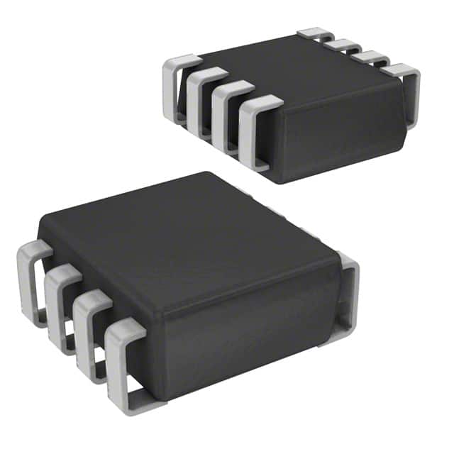
- Part No.:
- AAT4295IJS-T1
- Manufacturer:
- Skyworks Solutions Inc.
- Category:
- I/O Expanders
- Package:
- 8-TFSOJ (0.069", 1.75mm Width)
- Datasheet:
-
 AAT4295IJS-T1.pdf
- Description:
- IC XPNDR SERIAL SC70
- Quantity:
- Payment:

- Shipping:

Inventory:4,644
Please send an inquiry. Send us your inquiry, and we will respond immediately.
Product details
Overview
AAT4295IJS-T1 from Skyworks Solutions is a three-channel low-side N-channel MOSFET RGB LED controller IC designed for portable fashion lighting applications. It operates from 1.8V to 5.5V, delivers ≤6.0 Ω RDS(ON) at 5V, consumes 3 μA quiescent current in active mode, and uses a single GPIO S2Cwire™ interface to configure all outputs - enabling compact, GPIO-efficient designs in space-constrained mobile devices.
For engineers reviewing the AAT4295IJS-T1 datasheet, AAT4295IJS-T1 pinout, AAT4295IJS-T1 application, or AAT4295IJS-T1 equivalent, key selection criteria include its SC70JW-8 package footprint, 3-channel low-side switching architecture, S2Cwire serial control timing (≤75 μs latch timeout), thermal dissipation limit of 440 mW at 25°C, and compatibility with common-anode RGB LEDs requiring ground-switched current paths.
Technical Context
The AAT4295IJS-T1 integrates three independent low-side N-channel MOSFETs with gate drive logic controlled exclusively via the EN/SET pin using Skyworks' proprietary S2Cwire™ serial interface - no external clock or data lines required. Each switch supports continuous load currents up to 271 mA per channel at 25°C ambient when all channels are active, limited by package thermal resistance (θJA = 225°C/W) and RDS(ON) temperature coefficient (2800 ppm/°C).
It implements an 8-state internal counter decoded from rising edges on EN/SET, with default activation on first rising edge (all switches ON), and full shutdown (<1 μA supply current) when EN/SET is held low for ≥500 μs. The device requires no external components for basic operation and is rated for –40°C to +85°C industrial temperature range.
Key Specifications
| Parameter | Value and Actual Design Meaning |
|---|---|
| Supply Voltage Range | 1.8 V to 5.5 V - supports direct connection to Li-ion battery (2.8–4.2 V) or regulated 3.3/5 V rails without level-shifting. |
| RDS(ON) (Typical) | 1.9 Ω at VCC = 5 V - enables ≤271 mA per channel at 25°C before exceeding 440 mW package power limit. |
| Quiescent Current | 3 μA typical in enabled state - minimizes battery drain during active LED control in always-on lighting modes. |
| S2Cwire Timing | Latch timeout (TLAT) = 500 μs - defines maximum high-time on EN/SET needed to lock output configuration after pulse train. |
| Operating Temperature | –40°C to +85°C - qualified for use in consumer handhelds exposed to ambient thermal cycling and battery self-heating. |
| Package | SC70JW-8 (2.1 mm × 2.0 mm × 0.5 mm) - ultra-compact, Pb-free surface-mount package compatible with standard reflow profiles. |
| Switch Count | Three independent low-side N-MOSFETs - provides discrete control of R, G, B LED cathodes in common-anode configurations. |
Pinout & Package
Package: SC70JW-8 (8-pin, 2.1 mm × 2.0 mm, 0.5 mm height, Pb-free, moisture-sensitive level 1).
| Pin/Terminal | Circuit Role | Design Meaning |
|---|---|---|
| 1 | VCC | Main power input - supplies internal logic and MOSFET gates; must be bypassed with 0.1 μF ceramic capacitor near pin. |
| 2, 3 | N/C | No internal connection - left unconnected; no PCB trace or pad required. |
| 4 | EN/SET | S2Cwire serial control input - rising edges program output states; logic low for ≥500 μs disables all switches and reduces IQ to <1 μA. |
| 5 | GND | Ground reference for power and signal - must be low-impedance connection to system ground plane. |
| 6 | S1 | Drain of Channel 1 MOSFET - connects load (e.g., red LED cathode) to ground when enabled; rated for ≤271 mA continuous. |
| 7 | S2 | Drain of Channel 2 MOSFET - independently controllable drain for green LED cathode or other low-side load. |
| 8 | S3 | Drain of Channel 3 MOSFET - independently controllable drain for blue LED cathode or auxiliary load switching. |
Key Features
| Feature | Design Value |
|---|---|
| Single-GPIO S2Cwire™ Interface | Eliminates need for three separate MCU GPIOs - reduces routing congestion and firmware complexity in tight-layout mobile PCBs. |
| No External Components Required | Operates stand-alone with only VCC, GND, EN/SET, and load connections - cuts BOM count and assembly cost vs. discrete MOSFET + resistor solutions. |
| Ultra-Low Quiescent Current | 3 μA active mode / <1 μA shutdown - extends battery life in always-on fashion lighting features without compromising responsiveness. |
| Thermally Optimized SC70JW Package | 225°C/W θJA enables 440 mW max power dissipation at 25°C - supports higher LED brightness than comparable 8-pin packages. |
| Robust Input Voltage Range | 1.8–5.5 V operation - interfaces directly with Li-ion batteries (2.8–4.2 V), 3.3 V logic, or 5 V USB-powered systems without regulators. |
Applications
| RGB Fashion Lighting | Keypad Backlighting |
|---|---|
|
Use Scenario: Dynamic color-changing illumination on smartphone bezels or wearable device housings using common-anode RGB LEDs. IC Role / Device Role / Timing Role: Low-side switch controlling R/G/B LED cathodes; S2Cwire enables rapid color transitions (<1 ms) via pulse-count sequencing. Use Value: Replaces three discrete MOSFETs + GPIOs with one IC, reducing layout area by >60% and eliminating gate-drive resistor matching. |
Use Scenario: Adjustable-intensity backlight for membrane keypads in portable medical or industrial handhelds. IC Role / Device Role / Timing Role: Independent channel control allows dimming individual keys or zones; EN/SET pulse count sets brightness level per segment. Use Value: Enables multi-level backlighting with single MCU pin - avoids PWM generator hardware or software timer overhead. |
| Display Sub-Backlight Control | Indicator Lamp Sequencing |
|
Use Scenario: Secondary LCD or OLED sub-display backlight in foldable phones or dual-screen tablets. IC Role / Device Role / Timing Role: Three-channel switching drives white LED strings or RGB segments; thermal design supports sustained 20–30 mA/channel operation. Use Value: Provides dedicated, low-noise switching without loading main display power rail - improves EMI margin and display contrast stability. |
Use Scenario: Status indication on IoT sensors or smart home hubs using discrete red/green/blue indicator LEDs. IC Role / Device Role / Timing Role: Configurable ON/OFF states per channel allow unique blink patterns (e.g., solid red = error, flashing green = pairing). Use Value: Eliminates need for microcontroller firmware to manage multiple LED timers - state is retained in hardware until next EN/SET pulse. |
Equivalent & Alternatives
The following parts are listed as comparable options for similar low-side RGB LED switching applications.
| Alternative Part | Technical Difference | Application Difference | Selection Advice |
|---|---|---|---|
| Texas Instruments TPS22965DSGR | Single-channel, 0.85 Ω RDS(ON), 1.65–5.5 V, no serial interface - requires separate GPIO per channel. | Not suitable for RGB sequencing; best for fixed-function single-load switching where size is secondary to on-resistance. | Select if lowest possible RDS(ON) is critical and MCU has spare GPIOs; avoid if S2Cwire simplification or multi-channel coordination is needed. |
| Diodes Incorporated AP22851W5-7 | Triple-channel, 3.5 Ω RDS(ON) at 5 V, enable-only control (no programmable states), 1.8–5.5 V. | Supports simultaneous ON/OFF only - cannot sequence individual channels or implement color mixing via pulse count. | Choose for cost-sensitive designs needing basic triple-switch functionality without sequencing; not viable for dynamic RGB lighting effects. |
Compared with TPS22965DSGR and AP22851W5-7, the AAT4295IJS-T1 uniquely combines three-channel integration, S2Cwire serial programming, and sub-2 Ω RDS(ON) in an SC70JW-8 package - delivering superior GPIO efficiency and lighting flexibility without sacrificing thermal performance or voltage range.
Availability
AAT4295IJS-T1 is available at Aetrix Electronics and suitable for RGB fashion lighting, keypad backlighting, and indicator lamp control requiring stable component supply across consumer electronics production cycles.
Supply support for AAT4295IJS-T1 includes scheduled delivery planning, volume procurement assistance, BOM continuity management, traceable sourcing, and lifecycle availability coordination for OEM customers, industrial embedded developers, connected-device designers, and electronics production programs.
Manufacturer
Skyworks Solutions is a global semiconductor company specializing in analog and mixed-signal connectivity solutions for wireless, automotive, and industrial markets.
The AAT4295IJS-T1 belongs to Skyworks' Application Specific Power MOSFET (ASPM™) family, engineered to replace discrete MOSFET+driver combinations in portable LED lighting systems where space, power efficiency, and GPIO conservation are critical.
FAQ
What is the maximum continuous current per channel for the AAT4295IJS-T1?
The AAT4295IJS-T1 supports up to 271 mA per channel at 25°C ambient when all three switches are active, calculated from its 440 mW maximum package power dissipation and typical RDS(ON) of 1.9 Ω at 5 V. At 85°C ambient, this drops to ~133 mA per channel due to thermal derating. The AAT4295IJS-T1 datasheet specifies absolute maximum drain current per switch as limited by package thermal capability, not intrinsic MOSFET rating.
Does the AAT4295IJS-T1 require external pull-up resistors on the EN/SET line?
No, the AAT4295IJS-T1 does not require external pull-up resistors on the EN/SET line. Its internal circuitry accepts direct GPIO connection, and the datasheet explicitly states that EN/SET "should not be left floating" - implying internal biasing exists. The S2Cwire interface relies on controlled rising-edge pulses, not steady-state logic levels, so external pull-ups would interfere with pulse timing integrity. The AAT4295IJS-T1 functions correctly with a standard CMOS GPIO driving EN/SET directly.
Can the AAT4295IJS-T1 drive common-cathode RGB LEDs?
No, the AAT4295IJS-T1 is designed exclusively for common-anode RGB LED configurations. As a low-side switch, it connects LED cathodes to ground - requiring the anodes to be tied to a positive supply. Driving common-cathode LEDs would require high-side switching, which the AAT4295IJS-T1 does not support. Attempting to use it with common-cathode LEDs results in no current flow. The AAT4295IJS-T1 application circuits and functional description in the Skyworks datasheet confirm its intended use with common-anode topologies.
What is the minimum pulse width required for reliable S2Cwire communication with the AAT4295IJS-T1?
The AAT4295IJS-T1 requires a minimum EN/SET high time (TEN/SET_HI_MIN) of 50 ns and a maximum high time (TEN/SET_HI_MAX) of 75 μs per pulse for valid S2Cwire decoding. Pulses shorter than 50 ns may not register as rising edges; pulses longer than 75 μs trigger the 500 μs latch timeout, causing premature state locking. The AAT4295IJS-T1 datasheet specifies these timing constraints in the Electrical Characteristics table and confirms reliable operation up to 1 MHz clock rates when adhering to these bounds.
Is the AAT4295IJS-T1 pin-compatible with the AAT4297?
No, the AAT4295IJS-T1 is not pin-compatible with the AAT4297. The AAT4295IJS-T1 uses an 8-pin SC70JW package with pins assigned to VCC, two N/C, EN/SET, GND, and three switch drains (S1–S3). The AAT4297 uses a 12-pin TSOPJW package with six switch drains (S1–S6), additional N/C pins, and different pin spacing. Their pin configurations, counts, and footprints are mutually incompatible - PCB layout redesign is required to substitute one for the other. The AAT4295IJS-T1 datasheet explicitly lists separate pinouts and packages for each device.
AAT4295IJS-T1 Specifications
- Product attributes
- Attribute value
- Manufacturer:
- Skyworks Solutions Inc.
- Series:
- -
- Package/Case:
- 8-TFSOJ (0.069", 1.75mm Width)
- Packaging:
- Tape & Reel (TR)
- Product Status:
- Obsolete
- Programmable:
- Not Verified
- Number of I/O:
- 3
- Interface:
- Serial
- Interrupt Output:
- No
- Features:
- -
- Output Type:
- -
- Current - Output Source/Sink:
- -
- Clock Frequency:
- -
- Voltage - Supply:
- 1.8V ~ 5.5V
- Operating Temperature:
- -40°C ~ 85°C
- Grade:
- -
- Qualification:
- -
- Mounting Type:
- Surface Mount
- Supplier Device Package:
- 8-SC70JW
AAT4295IJS-T1 FAQ
1.How can I place an order for AAT4295IJS-T1 through Aetrix?
Please submit a Request for Quotation (RFQ) for AAT4295IJS-T1 on Aetrix. Our sales agent will provide a competitive quotation and guide you through the order confirmation once you accept the terms.
2.Are the price and stock information for AAT4295IJS-T1 reliable?
The price and inventory of AAT4295IJS-T1 are updated periodically and may fluctuate due to market conditions. Stock and pricing data are typically refreshed every 24 hours. Quotation validity for AAT4295IJS-T1 is usually 5 days.
3.What payment methods are accepted for AAT4295IJS-T1?
We accept Wire Transfer, PayPal, Credit Card, Western Union, MoneyGram, and Escrow for AAT4295IJS-T1 transactions.
Note: Certain payment methods may incur a processing fee.
4.How is shipping managed for AAT4295IJS-T1?
AAT4295IJS-T1 orders can be shipped via leading logistics carriers, including DHL, UPS, FedEx, TNT, or Registered Mail.
Once your AAT4295IJS-T1 order is processed, you will receive an email with the shipment details and tracking number.
Note: Tracking information may take up to 24 hours to appear. Express delivery typically takes 3–5 business days.
5.How can I obtain technical support or documentation for AAT4295IJS-T1?
For technical support, including AAT4295IJS-T1 datasheets, pinout diagrams, or application guidance, please contact our engineering support team. They can provide detailed documentation and assistance for your AAT4295IJS-T1 requirements.
6.How does Aetrix verify that AAT4295IJS-T1 is sourced from the original manufacturer or authorized distributors?
All AAT4295IJS-T1 products on Aetrix are procured from qualified distributors and authorized channels. Our dedicated quality assurance team conducts strict verification, including traceability checks and, if necessary, third-party testing. This ensures that AAT4295IJS-T1 meets industry standards.
7.What is the process for return or replacement of AAT4295IJS-T1?
All AAT4295IJS-T1 units undergo pre-shipment inspection (PSI). If there is an issue with AAT4295IJS-T1, returns or replacements are accepted under the following conditions:
1.Quantity discrepancies, incorrect items, or visible external defects (such as breakage or corrosion), acknowledged by Aetrix.
2.The issue is reported within 90 days of delivery.
3.The AAT4295IJS-T1 part is unused and in its original packaging.
Return procedure for AAT4295IJS-T1:
1.Submit a request within 90 days.
2.Obtain a Return Material Authorization (RMA) from Aetrix.
AAT4295IJS-T1 Tags
-
TCA6408ARSVR
Texas Instruments

-
TCA9535RTWR
Texas Instruments
-
FXL6408UMX
onsemi

-
PCF8574ADWR
Texas Instruments

-
PCF8574APWR
Texas Instruments
-
TCA9555PWR
Texas Instruments

-
TCA9554PWR
Texas Instruments
-
TCA9554APWR
Texas Instruments

-
TCA9539PWR
Texas Instruments
-
TCA9534PWR
Texas Instruments
-
TCA9555RTWR
Texas Instruments
-
TCA9535PWR
Texas Instruments
Tech Hub

Counterfeit components can hide behind convincing markings and passing basic function tests. This engineering reference covers source traceability, external inspection, X-ray, XRF, electrical testing, …

A practical engineering and sourcing framework covering lifecycle verification, lifetime-buy calculations, replacement qualification, supplier checks and counterfeit-risk controls.

TTL and CMOS logic families differ in thresholds, loading, output drive, power and timing. This engineering guide compares 74HC and 74HCT, calculates noise margins and checks 3.3 V/5 V compatibility.

A practical engineering guide to 3.3V and 5V logic compatibility, input thresholds, resistor dividers, translator ICs, MOSFET level shifting, I2C pull-ups, timing limits and power-sequencing risks.

The 74HC595 uses push-pull logic outputs, while the TPIC6B595 uses 50 V open-drain DMOS sinks for higher-power loads. This guide compares timing, current limits, 3.3 V interfacing, load wiring, thermal…

The 74HC595 converts serial data into eight stable parallel outputs. This guide covers pin functions, shift and storage timing, OE and MR behavior, drive-current limits, cascading, voltage compatibilit…

A technical comparison of level-sensitive latches and edge-triggered flip-flops, covering timing windows, setup and hold limits, master–slave operation, time borrowing, race-through, HDL inference and…

A D latch stores one bit while Enable controls when data can pass. This reference covers gate-level operation, truth tables, transparency, setup and hold timing, LE versus OE, common ICs and practical …

An SR latch stores one bit through cross-coupled feedback. This engineering reference covers NOR and NAND implementations, truth tables, forbidden-state recovery, gated operation, switch debouncing, fa…

Latch circuits retain one bit through feedback. This technical reference covers SR and D latches, truth tables, transparency, timing limits, latch-versus-flip-flop behavior, applications and common log…


