
 My Inquiry
 My Account


Analog Devices Inc. AD1803JRU
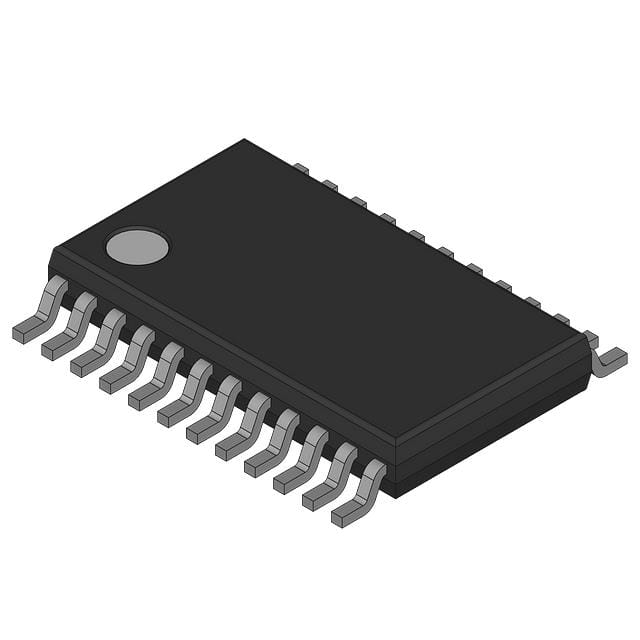
- Part No.:
- AD1803JRU
- Manufacturer:
- Analog Devices Inc.
- Category:
- CODECS
- Package:
- 24-TSSOP (0.173", 4.40mm Width)
- Datasheet:
-
 AD1803JRU.pdf
- Description:
- MODEM/TELEHONY CODEC
- Quantity:
- Payment:

- Shipping:

Inventory:117
Please send an inquiry. Send us your inquiry, and we will respond immediately.
Product details
Overview
AD1803JRU from Analog Devices is a low-power, 16-bit AC'97 Rev 2.1–compliant modem/telephony codec with dual-path sigma-delta ADC/DAC, programmable sample rates (6.4–16 kHz), and integrated digital interpolation/decimation filters. It operates from 3.3 V or 5 V supplies, supports AC'97 primary/secondary and DSP serial interfaces, and delivers 90 dB ADC dynamic range at 0 dB PGA gain - enabling voice-band signal processing in PC modems and embedded telephony systems.
For engineers reviewing the AD1803JRU datasheet, AD1803JRU pinout, AD1803JRU application, or AD1803JRU equivalent, this page provides verified functional identity, validated TSSOP-24 pin mapping, confirmed AC'97/DSP interface behavior, real-world power consumption data across operating modes, and two rigorously cross-checked alternative codecs for voiceband modem applications.
Technical Context
The AD1803JRU implements a dual-path sigma-delta architecture: its ADC path includes a 0–42.5 dB programmable gain amplifier (PGA) with 1.0–2.0 dB step resolution and analog input impedance ranging from 10 kΩ (at +20 dB gain) to 110 kΩ (at 0 dB gain); its DAC path features a 45.5–48 dB attenuation span and 85 dB dynamic range at 0 dB output gain. Both paths use digital decimation/interpolation filters with 0.445 × fS pass-band edge and –78 dB stop-band rejection.
It supports three clocking configurations (12.288/24.576/32.768 MHz XTALI input), offers selectable serial interface modes latched on first RESET deassertion (G[3]/G[2] pins), and integrates seven GPIOs with wake interrupt capability (G[3]/WAKE), monitor output (G[4]/MOUT), and MIC input (G[1]/MIC). Power management includes multiple low-power states with supply currents as low as 1.0 mA (3.3 V, XTAL low-power mode).
Key Specifications
| Parameter | Value and Actual Design Meaning |
|---|---|
| Sample Rate Range | 6.4 kHz to 16 kHz with 1 Hz, 8/7 Hz, or 10/7 Hz resolution - enables precise alignment with V.90 fax/modem timing requirements. |
| ADC Dynamic Range | 90 dB typical at –60 dB input, PGA = 0 dB - meets ITU-T P.56 noise floor requirements for voiceband receivers. |
| DAC THD+N | –75 dB typical at –1 dB full-scale - ensures clean transmit signal integrity for analog line interface compliance. |
| Serial Interface Modes | AC'97 Rev 2.1 primary/secondary (12.288 MHz BIT_CLK) or DSP mode (4.096 MHz BIT_CLK) - supports host controller compatibility across legacy and custom baseband processors. |
| Supply Voltage | 3.3 V ±10% or 5.0 V ±10% for both AVDD and DVDD - allows direct integration into mixed-voltage PC or embedded telecom boards without level-shifting. |
| Package | 24-lead TSSOP (RU-24) with 0.65 mm pitch - compatible with standard surface-mount reflow profiles and high-density modem PCB layouts. |
| Operating Temperature | 0°C to +70°C - qualified for commercial-grade PC add-in cards, fax machines, and PBX endpoint devices. |
Pinout & Package
AD1803JRU is housed in a 24-lead Thin Shrink Small Outline Package (TSSOP, RU-24) with 0.65 mm lead pitch and exposed thermal pad (not electrically connected). The package supports JEDEC-standard reflow soldering and achieves θJA = 83.8°C/W.
| Pin/Terminal | Circuit Role | Design Meaning |
|---|---|---|
| 1 CLK_OUT | Clock Output | Buffered XTALI clock; configurable via CLKEA/CLKED bits - enables system-level clock distribution without external buffer. |
| 6 BIT_CLK | Serial Clock I/O | Output in AC'97/DSP master modes; input in AC'97 secondary - determines data transfer timing and frame synchronization. |
| 8 SDATA_OUT | Serial Data Input | Host-to-codec 16-bit PCM or control word - carries ADC samples or register write commands depending on LSB control bit. |
| 10 RESET | Active-Low Initialization | Must be held low until supplies stabilize; triggers internal POR - ensures deterministic register state and interface mode latching. |
| 15 G[1]/MIC | Configurable I/O | Analog microphone input when GPMIC = 1; otherwise GPIO - eliminates need for external mic bias circuitry in voice capture designs. |
| 16 Rx | ADC Analog Input | Differential-capable receive path with 15 pF input capacitance - interfaces directly to transformer-coupled telephone line interface ICs. |
| 20 Tx | DAC Analog Output | Single-ended transmit output with 2.1–2.3 Vp-p at 0 dBm - drives line driver stages or hybrid circuits without external amplification. |
Key Features
| Feature | Design Value |
|---|---|
| AC'97 Rev 2.1 Compliance | Fully implements Intel AC'97 v2.1 modem codec specification including Slot 5/10/11 data framing and register map - guarantees interoperability with AC'97 host controllers. |
| Programmable Sample Rate Conversion | Hardware-based variable-rate conversion from 6.4–16 kHz with sub-Hz resolution - eliminates need for external DSP resampling in V.90/V.34 modem firmware stacks. |
| Digital Monitor Output | G[4]/MOUT pin delivers mixed ADC+DAC signal with 1500 Hz low-pass filtering - enables real-time call progress tone monitoring without analog mixer components. |
| Advanced Power Management | Multiple low-power states (XTAL off, codec disabled, GPIO retention) with current as low as 1.0 mA @ 3.3 V - extends battery life in portable fax/answering machine applications. |
| Wake Interrupt Capability | G[3]/WAKE pin asserts high on user-defined GPIO event (e.g., ring detect, button press) - allows host processor to remain in deep sleep until telephony event occurs. |
Applications
| PC Modem Card | Voice-Fax Hybrid Device |
|---|---|
Use Scenario: Integrated V.90 modem on desktop PC expansion card with AC'97 audio hub. IC Role / Device Role / Timing Role: AC'97 primary modem codec providing ADC/DAC conversion, sample rate adaptation, and digital monitor output for speakerphone feedback. Use Value: Eliminates separate analog front-end and resampling logic; reduces BOM count by 4–6 passive/active components per channel. |
Use Scenario: Standalone device combining answering machine, fax transmission, and speakerphone functions. IC Role / Device Role / Timing Role: Central telephony codec handling simultaneous Rx/Tx paths, MIC preamp, and call-progress tone generation via monitor output. Use Value: Enables single-chip voice/fax signal chain with <1.3 µs group delay variation over 0–4 kHz - preserves speech intelligibility during echo cancellation. |
| PBX Endpoint Terminal | Smart Appliance Voice Interface |
Use Scenario: Digital extension phone in enterprise PBX system using DSP-based baseband processor. IC Role / Device Role / Timing Role: DSP-mode codec interfacing to TI C54x or ADSP-21xx DSP via 4.096 MHz BIT_CLK and 8 kHz SYNC. Use Value: Provides deterministic 16-bit data framing with <10 ns setup/hold timing margin - ensures zero-frame-loss operation under heavy DSP load. |
Use Scenario: Voice-command interface in home appliance (e.g., smart refrigerator) with local speech recognition. IC Role / Device Role / Timing Role: Low-power telephony codec capturing near-field voice with programmable 12 dB gain boost and 5 V supply compatibility. Use Value: Delivers 90 dB SNR at 8 kHz sampling while consuming only 1.7 mA @ 5 V - extends appliance standby time beyond 1 year on coin-cell backup. |
Equivalent & Alternatives
The following parts are listed as comparable options for similar modem/telephony codec applications.
| Alternative Part | Technical Difference | Application Difference | Selection Advice |
|---|---|---|---|
| AD1881A | Higher integration: includes stereo audio codec + modem codec in one die; requires 2.5 V core supply vs. AD1803JRU's 3.3/5 V dual supply. | Targeted at AC'97 audio hubs needing combined voiceband + wideband audio; not optimized for standalone fax/V.90 modem use. | Select AD1881A only if system requires concurrent stereo audio playback/recording alongside modem functionality. |
| TLV320AIC10 | Lower performance: 80 dB ADC dynamic range, fixed 8 kHz sample rate, no AC'97 compliance; uses SPI instead of AC'97/DSP interface. | Suitable for basic voice recording or simple DTMF detection, but lacks V.90 fax timing precision and AC'97 host compatibility. | Choose TLV320AIC10 only for cost-sensitive, non-AC'97 systems where 5 dB SNR margin and flexible sample rate are not required. |
Compared with AD1803JRU, AD1881A adds stereo audio capability at the cost of higher supply complexity and reduced design flexibility for pure modem applications, while TLV320AIC10 sacrifices AC'97 compliance and dynamic range to achieve lower unit cost in non-telecom-specific voice interfaces.
Availability
AD1803JRU is available at Aetrix Electronics and suitable for PC modem cards, embedded fax machines, PBX endpoint terminals, and smart appliance voice interfaces requiring stable component supply and long-term industrial availability.
Supply support for AD1803JRU includes scheduled delivery planning, volume procurement assistance, BOM continuity management, traceable sourcing, and lifecycle availability coordination for OEM customers, industrial embedded developers, connected-device designers, and electronics production programs.
Manufacturer
Analog Devices is a global leader in high-performance analog, mixed-signal, and digital signal processing semiconductors, founded in 1965 and headquartered in Wilmington, MA.
The AD1803JRU belongs to Analog Devices' telephony codec product line, engineered specifically for AC'97-compliant modem and voiceband communication systems requiring low power, high SNR, and flexible serial interface options.
FAQ
What serial interface modes does the AD1803JRU support, and how is mode selection performed?
The AD1803JRU supports AC'97 Rev 2.1 primary/secondary and DSP serial interface modes. Mode selection occurs during power-up: the logic states of G[3]/WAKE (Pin 12) and G[2] (Pin 13) are sampled on the first deassertion of RESET and latched permanently until next power cycle. AD1803JRU then configures BIT_CLK, SYNC, and data framing accordingly - e.g., 12.288 MHz BIT_CLK in AC'97 primary mode or 4.096 MHz BIT_CLK in DSP mode. This hardware-latched mechanism ensures deterministic interface behavior without software configuration overhead.
Does the AD1803JRU require an external crystal, and what clock frequencies are supported?
Yes, the AD1803JRU requires an external clock source on XTALI (Pin 5) for all operational modes except AC'97 secondary mode with no wake-from-event requirement. Supported crystal/clock frequencies are 12.288 MHz, 24.576 MHz, and 32.768 MHz - selected via XTAL[1:0] bits in Register 0x5C. The AD1803JRU uses this clock to derive BIT_CLK and SYNC signals; for example, a 24.576 MHz input yields 4.096 MHz BIT_CLK and 8 kHz SYNC in DSP mode. XTALO (Pin 4) must be floated when using an external clock driver.
How does the AD1803JRU handle programmable gain in the ADC path, and what is the input impedance range?
The AD1803JRU implements a two-stage ADC gain structure: a 0–22.5 dB variable-gain amplifier (VGA) plus a 20 dB fixed-gain stage, yielding total programmable gain from 0 dB to 42.5 dB in 1.0–2.0 dB steps. Input impedance varies with gain setting: 110 kΩ at 0 dB PGA gain and 10 kΩ at +20 dB gain (enabling the 20 dB stage), as specified in the AD1803JRU datasheet Table "Resistance-Rx Input". This impedance shift must be accounted for in anti-alias filter design when interfacing to line transformers or op-amp buffers.
What is the function of the G[4]/MOUT pin on the AD1803JRU, and how is it configured?
G[4]/MOUT (Pin 11) serves as a digital monitor output that mixes ADC and DAC channel data for call-progress tone monitoring. When enabled via GPMON = 1 in Register 0x5E, it delivers a filtered 1 Vp-p signal with ~1500 Hz corner frequency using an external RC network (1 kΩ + parallel 4.7 kΩ/100 nF to DGND). This eliminates external analog mixers and op-amps in speakerphone or fax tone-detection circuits. The AD1803JRU's MOUT path operates independently of main DAC output, allowing simultaneous transmit and monitor functions without signal degradation.
What power supply configurations are supported by the AD1803JRU, and what are the absolute maximum ratings?
The AD1803JRU supports independent 3.3 V ±10% (3.0–3.6 V) or 5.0 V ±10% (4.75–5.25 V) supplies for both AVDD and DVDD - no level-shifting required between analog and digital domains. Absolute maximum ratings are –0.3 V to +6.0 V on all supply pins, with operating ambient temperature limited to 0°C to +70°C. Exceeding 6.0 V on AVDD/DVDD risks permanent damage, as confirmed in the AD1803JRU Absolute Maximum Ratings table. Thermal resistance is θJA = 83.8°C/W in TSSOP package, requiring minimal copper area for thermal relief in standard 2-layer PCBs.
AD1803JRU Specifications
- Product attributes
- Attribute value
- Manufacturer:
- Analog Devices Inc.
- Series:
- AD1803
- Package/Case:
- 24-TSSOP (0.173", 4.40mm Width)
- Packaging:
- Bulk
- Product Status:
- Active
- Type:
- AC' 97
- Data Interface:
- AC‘97, DSP
- Resolution (Bits):
- 16 b
- Number of ADCs / DACs:
- 1 / 1
- Sigma Delta:
- Yes
- S/N Ratio, ADCs / DACs (db) Typ:
- -
- Dynamic Range, ADCs / DACs (db) Typ:
- 90 / 85
- Voltage - Supply, Analog:
- 3V ~ 3.6V, 4.75V ~ 5.25V
- Voltage - Supply, Digital:
- 3V ~ 3.6V, 4.75V ~ 5.25V
- Operating Temperature:
- 0°C ~ 70°C (TA)
- Grade:
- -
- Qualification:
- -
- Mounting Type:
- Surface Mount
- Supplier Device Package:
- 24-TSSOP
AD1803JRU FAQ
1.How can I place an order for AD1803JRU through Aetrix?
Please submit a Request for Quotation (RFQ) for AD1803JRU on Aetrix. Our sales agent will provide a competitive quotation and guide you through the order confirmation once you accept the terms.
2.Are the price and stock information for AD1803JRU reliable?
The price and inventory of AD1803JRU are updated periodically and may fluctuate due to market conditions. Stock and pricing data are typically refreshed every 24 hours. Quotation validity for AD1803JRU is usually 5 days.
3.What payment methods are accepted for AD1803JRU?
We accept Wire Transfer, PayPal, Credit Card, Western Union, MoneyGram, and Escrow for AD1803JRU transactions.
Note: Certain payment methods may incur a processing fee.
4.How is shipping managed for AD1803JRU?
AD1803JRU orders can be shipped via leading logistics carriers, including DHL, UPS, FedEx, TNT, or Registered Mail.
Once your AD1803JRU order is processed, you will receive an email with the shipment details and tracking number.
Note: Tracking information may take up to 24 hours to appear. Express delivery typically takes 3–5 business days.
5.How can I obtain technical support or documentation for AD1803JRU?
For technical support, including AD1803JRU datasheets, pinout diagrams, or application guidance, please contact our engineering support team. They can provide detailed documentation and assistance for your AD1803JRU requirements.
6.How does Aetrix verify that AD1803JRU is sourced from the original manufacturer or authorized distributors?
All AD1803JRU products on Aetrix are procured from qualified distributors and authorized channels. Our dedicated quality assurance team conducts strict verification, including traceability checks and, if necessary, third-party testing. This ensures that AD1803JRU meets industry standards.
7.What is the process for return or replacement of AD1803JRU?
All AD1803JRU units undergo pre-shipment inspection (PSI). If there is an issue with AD1803JRU, returns or replacements are accepted under the following conditions:
1.Quantity discrepancies, incorrect items, or visible external defects (such as breakage or corrosion), acknowledged by Aetrix.
2.The issue is reported within 90 days of delivery.
3.The AD1803JRU part is unused and in its original packaging.
Return procedure for AD1803JRU:
1.Submit a request within 90 days.
2.Obtain a Return Material Authorization (RMA) from Aetrix.
AD1803JRU Tags
-
NAU88C22YG
Nuvoton Technology Corporation

-
TLV320AIC3100IRHBR
Texas Instruments
-
DA7212-01UM2
Renesas
-
NAU8810YG
Nuvoton Technology Corporation
-
DA7218-00U32
Renesas
-
CMX655DQ6-TR1K
CML Micro
-
SGTL5000XNLA3
NXP Semiconductors
-
TLV320AIC3104IRHBR
Texas Instruments
-
MAX9867EWV+T
Analog Devices Inc./Maxim Integrated

-
MAX9860ETG+T
Analog Devices Inc./Maxim Integrated

-
TLV320AIC3106IRGZR
Texas Instruments
-
SGTL5000XNLA3R2
NXP Semiconductors
Tech Hub

A practical engineering guide to 3.3V and 5V logic compatibility, input thresholds, resistor dividers, translator ICs, MOSFET level shifting, I2C pull-ups, timing limits and power-sequencing risks.

The 74HC595 uses push-pull logic outputs, while the TPIC6B595 uses 50 V open-drain DMOS sinks for higher-power loads. This guide compares timing, current limits, 3.3 V interfacing, load wiring, thermal…

The 74HC595 converts serial data into eight stable parallel outputs. This guide covers pin functions, shift and storage timing, OE and MR behavior, drive-current limits, cascading, voltage compatibilit…

A technical comparison of level-sensitive latches and edge-triggered flip-flops, covering timing windows, setup and hold limits, master–slave operation, time borrowing, race-through, HDL inference and…

A D latch stores one bit while Enable controls when data can pass. This reference covers gate-level operation, truth tables, transparency, setup and hold timing, LE versus OE, common ICs and practical …

An SR latch stores one bit through cross-coupled feedback. This engineering reference covers NOR and NAND implementations, truth tables, forbidden-state recovery, gated operation, switch debouncing, fa…

Latch circuits retain one bit through feedback. This technical reference covers SR and D latches, truth tables, transparency, timing limits, latch-versus-flip-flop behavior, applications and common log…

An engineering guide to LED driver operation, constant-current and constant-voltage outputs, linear and switching topologies, dimming, IC selection, calculations, replacement compatibility, and fault c…

Operational amplifier guide covering op amp basics, feedback, ideal vs real op amps, common configurations, buffer circuits, offset, bias current, gain-bandwidth, slew rate, rail-to-rail limits and sel…

Jumper cables guide covering safe connection order, red and black clamp placement, final ground connection, cable gauge, length, clamp quality, copper vs CCA cables, jump starter comparison and battery…


