
 My Inquiry
 My Account


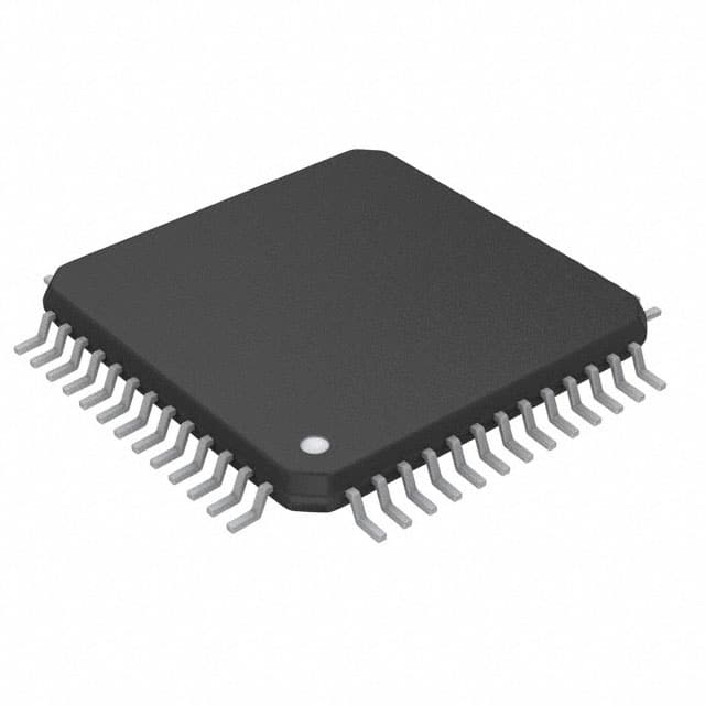
Analog Devices Inc. AD1839AAS
- Part No.:
- AD1839AAS
- Manufacturer:
- Analog Devices Inc.
- Category:
- CODECS
- Package:
- 52-QFP
- Datasheet:
-
 AD1839AAS.pdf
- Description:
- IC CODEC 2ADC/6DAC 24BIT 52-MQFP
- Quantity:
- Payment:

- Shipping:

Inventory:5,140
Please send an inquiry. Send us your inquiry, and we will respond immediately.
Product details
Overview
AD1839AAS from Analog Devices is a high-performance 24-bit sigma-delta audio codec integrating two stereo ADCs and three stereo DACs (six total DAC channels) in a single 52-lead MQFP package. It supports up to 96 kHz sample rates on all converters, with one DAC channel capable of 192 kHz operation, and delivers 105 dB SNR (ADC) and 108 dB SNR (DAC) for professional-grade audio capture and playback in home theater receivers and automotive infotainment systems.
For engineers reviewing the AD1839AAS datasheet, AD1839AAS pinout, AD1839AAS application, or AD1839AAS equivalent, key selection considerations include its 3.3 V–tolerant digital interface, independent 1024-step volume control per DAC channel, software-controllable clickless mute, TDM support for 8-in/8-out operation via SHARC SPORT, and on-chip 2.25 V reference with FILTD/FILTR filter capacitor terminals.
Technical Context
The AD1839AAS implements multibit Σ-∆ modulation in both ADC and DAC paths, with patented differential linearity restoration to suppress idle tones and reduce noise floor. Its ADC section uses decimation filters with 120 dB stop-band attenuation and linear phase response at 48 kHz and 96 kHz sample rates, while DAC interpolation filters provide ±0.01 dB pass-band ripple and group delays of 340 µs (48 kHz) and 160 µs (96 kHz).
Digital interface flexibility includes I²S-, left-justified, right-justified, and DSP-compatible serial modes plus auxiliary TDM mode supporting 256×/512× fS clocking. Control is handled via an SPI-compatible serial port (CCLK/CIN/CLATCH/COUT), and master/slave configuration for ADC clocks is selected via the M/S pin tied to ODVDD or DGND.
Key Specifications
| Parameter | Value and Actual Design Meaning |
|---|---|
| ADC Channels | 2 stereo (4-channel differential input) |
| DAC Channels | 3 stereo (6 single-ended voltage outputs) |
| Max Sample Rate | 96 kHz on all converters; 192 kHz on DAC1 only |
| Resolution | 24-bit for both ADC and DAC paths |
| SNR / Dynamic Range | ADC: 105 dB A-weighted; DAC: 108 dB A-weighted |
| THD + N | ADC: −95 dB; DAC: −92 dB (at 48/96 kHz) |
| Volume Control | 1024-step linear scale per DAC channel, 60 dB range |
| Package | 52-lead MQFP, −40°C to +85°C industrial temperature range |
Pinout & Package
AD1839AAS is housed in a 52-lead MQFP (Metric Quad Flat Package) with exposed thermal pad, specified for industrial temperature operation (−40°C to +85°C). Pin functions are validated per Analog Devices Rev. B datasheet Figure 3 and Table 5.
| Pin/Terminal | Circuit Role | Design Meaning |
|---|---|---|
| DVDD (Pins 1, 39) | Digital power supply | 5 V supply for digital logic; requires local 100 nF bypass |
| AVDD (Pins 11, 19, 29) | Analog power supply | 5 V supply for analog sections; separate from DVDD for noise isolation |
| ODVDD (Pin 48) | Digital output driver supply | 3.0 V to DVDD range; enables 3.3 V–tolerant interface with external controllers |
| AGND (Pins 5, 10, 16, 24, 30, 34) | Analog ground | Must be isolated from DGND; star-ground connection recommended |
| DGND (Pins 40, 52) | Digital ground | Reference for digital I/O; separated from AGND to minimize coupling |
| MCLK (Pin 47) | Master clock input | Accepts 12.288 MHz (256× fS) or scaled variants; jitter <300 ps rms required |
| ABCLK / ALRCLK (Pins 45, 46) | ADC bit/frame clock | Configurable as input (slave) or output (master) via M/S pin |
| DBCLK / DLRCLK (Pins 38, 37) | DAC bit/frame clock | Supports normal, packed, and TDM modes; synchronous with DAC data |
| DSDATA1–3 (Pins 41–43) | DAC serial data inputs | Three independent stereo data streams; also supports TDM on DSDATA1 |
| ASDATA (Pin 49) | ADC serial data output | Time-multiplexed stereo output; format programmable via control registers |
| FILTD (Pin 17) | DAC bias filter terminal | Connect 10 µF/100 nF to ground to reduce DAC output noise |
| FILTR (Pin 18) | Reference filter terminal | Connect 10 µF/100 nF to ground to stabilize 2.25 V internal VREF |
| OUTL1/OUTR1 (Pins 7, 9) | DAC1 left/right outputs | Single-ended, 1.0 Vrms full-scale; dc-biased at VREF = 2.25 V |
| ADCLP/ADCLN (Pins 21, 20) | ADC left differential input | ±2.828 V differential range; common-mode voltage fixed at 2.25 V |
| PD/RST (Pin 4) | Power-down/reset input | Active-low; resets registers and initiates 20-LRCLK initialization sequence |
Key Features
| Feature | Design Value |
|---|---|
| Data-directed scrambling DACs | Minimizes sensitivity to clock jitter, enabling robust performance with low-cost oscillators |
| On-chip 2.25 V reference with FILTR | Provides stable bias for ADC inputs and DAC outputs; eliminates need for external reference |
| Clickless mute and volume control | Software-controlled per-channel muting and 0.098% step-size attenuation prevent audible transients |
| TDM interface mode | Enables 8-in/8-out audio routing over single SHARC SPORT, reducing interconnect complexity |
| Dual-supply architecture | Separate AVDD/DVDD/ODVDD pins allow clean analog domain and 3.3 V–compatible digital interfacing |
| Digital de-emphasis processing | Hardware-accelerated CD-standard de-emphasis (±0.1 dB gain error) reduces post-processing load |
Applications
| Home Theater Audio Receivers | DVD/Blu-ray Player Audio Processing |
|---|---|
Use Scenario: Multi-channel audio decoding and analog output for 5.1/7.1 surround sound systems with HDMI or S/PDIF input sources. IC Role / Device Role / Timing Role: Primary audio codec handling simultaneous ADC capture (microphone input) and DAC playback (surround channels) with precise sample rate alignment. Use Value: 108 dB DAC SNR ensures low-noise rear/surround channel output; TDM mode simplifies connection to multi-core audio DSPs. |
Use Scenario: High-fidelity stereo and multi-channel audio playback from optical or coaxial digital inputs in consumer disc players. IC Role / Device Role / Timing Role: Dual-role converter: ADC digitizes analog aux inputs (e.g., phono), while DACs drive line-level outputs with de-emphasis for legacy CD content. Use Value: Hardware de-emphasis and 24-bit resolution preserve original mastering intent; 192 kHz DAC1 supports high-res audio upsampling paths. |
| Automotive Infotainment Systems | Professional Audio Effects Processors |
Use Scenario: Central audio hub in vehicle head units managing Bluetooth streaming, AM/FM tuner, navigation voice prompts, and cabin mic input. IC Role / Device Role / Timing Role: System codec providing six DAC outputs for front/rear/subwoofer zones and dual ADC inputs for hands-free telephony and noise cancellation. Use Value: Independent 1024-step volume control per DAC channel enables zone-specific loudness compensation; −40°C to +85°C rating ensures reliability under hood conditions. |
Use Scenario: Real-time multi-effects processing in studio-grade rack units requiring low-latency analog I/O and flexible clocking. IC Role / Device Role / Timing Role: High-precision conversion engine synchronized to external word clock; supports variable sample rates (48/96 kHz) without reconfiguration. Use Value: 120 dB ADC stop-band attenuation prevents aliasing in oversampled effects algorithms; SPI control enables dynamic parameter updates during effect changes. |
Equivalent & Alternatives
The following parts are listed as comparable options for similar audio codec applications.
| Alternative Part | Technical Difference | Application Difference | Selection Advice |
|---|---|---|---|
| AK4384VN | 4-channel DAC only (no integrated ADC); 192 kHz native support across all channels | Lacks ADC functionality; requires external ADC for bidirectional audio paths | Select when system design separates ADC and DAC functions or prioritizes DAC channel count over integration |
| CS4272-CQZ | 2 ADC / 8 DAC channels; supports 192 kHz on all DACs; I²S-only interface (no TDM or DSP modes) | Higher DAC count but no auxiliary TDM or packed-mode flexibility; no 3.3 V–tolerant ODVDD pin | Prefer when maximum DAC channel density is critical and interface simplicity outweighs advanced clocking options |
Compared with AK4384VN and CS4272-CQZ, the AD1839AAS uniquely combines dual ADCs, six DACs, TDM capability, and 3.3 V–tolerant digital I/O in a single industrial-grade package-making it optimal for space-constrained, bidirectional audio systems requiring flexible clocking and hardware de-emphasis.
Availability
AD1839AAS is available at Aetrix Electronics and suitable for home theater receivers, automotive infotainment systems, and professional audio effects processors requiring stable component supply, long-term lifecycle support, and guaranteed industrial temperature performance.
Supply support for AD1839AAS includes scheduled delivery planning, volume procurement assistance, BOM continuity management, traceable sourcing, and lifecycle availability coordination for OEM customers, industrial embedded developers, connected-device designers, and electronics production programs.
Manufacturer
Analog Devices, Inc. is a global leader in high-performance analog, mixed-signal, and digital signal processing semiconductors, headquartered in Norwood, MA.
The AD1839AAS belongs to Analog Devices' precision audio codec product line, designed specifically for high-fidelity consumer and automotive audio systems demanding low THD+N, wide dynamic range, and flexible digital interface options.
FAQ
What is the maximum sample rate supported by the AD1839AAS for simultaneous ADC and DAC operation?
The AD1839AAS supports simultaneous 96 kHz operation on both its dual ADCs and all six DAC channels. While DAC1 can accept 192 kHz data, the ADC section is limited to 96 kHz maximum. For full-duplex 192 kHz systems, external ADCs must be used alongside AD1839AAS for the DAC path.
Does the AD1839AAS require external op amps for analog output filtering?
Yes-the AD1839AAS outputs single-ended signals with ±1.4 V swing around 2.25 V DC bias. Analog Devices recommends a third-order external low-pass op amp filter on each OUTLx/OUTRx pin to suppress out-of-band noise and prevent aliasing. Low-slew-rate op amps may cause high-frequency tones to fold into the audio band.
How is the AD1839AAS configured for TDM mode operation?
The AD1839AAS enters TDM mode via SPI register programming (TDM Enable bit in DAC Control 2 register). In TDM256 mode, it uses DSDATA1 for time-multiplexed 8-channel input/output with BCLK at 256× fS, FSTDM frame sync, and AUXBCLK for auxiliary data-enabling glueless connection to SHARC SPORT interfaces.
Can the AD1839AAS operate with a 3.3 V digital supply?
Yes-the AD1839AAS features a dedicated ODVDD pin (Pin 48) that accepts 3.0 V to DVDD (5 V), allowing direct interfacing with 3.3 V logic devices. DVDD remains at 5 V for digital core operation, while ODVDD powers only the output drivers, maintaining signal integrity and eliminating level-shifter requirements.
What is the function of the FILTD and FILTR pins on the AD1839AAS?
FILTD (Pin 17) connects to a grounded 10 µF/100 nF capacitor to reduce noise from the internal DAC bias circuitry. FILTR (Pin 18) serves the same purpose for the on-chip 2.25 V reference. Both capacitors are mandatory for achieving datasheet-spec SNR and THD+N performance; omitting them degrades dynamic range by up to 6 dB.
AD1839AAS Specifications
- Product attributes
- Attribute value
- Manufacturer:
- Analog Devices Inc.
- Series:
- -
- Package/Case:
- 52-QFP
- Packaging:
- Bag
- Product Status:
- Obsolete
- Type:
- Stereo Audio
- Data Interface:
- Serial
- Resolution (Bits):
- 24 b
- Number of ADCs / DACs:
- 2 / 6
- Sigma Delta:
- Yes
- S/N Ratio, ADCs / DACs (db) Typ:
- 105 / 108
- Dynamic Range, ADCs / DACs (db) Typ:
- 105 / 108
- Voltage - Supply, Analog:
- 4.5V ~ 5.5V
- Voltage - Supply, Digital:
- 4.5V ~ 5.5V
- Operating Temperature:
- -40°C ~ 85°C
- Grade:
- -
- Qualification:
- -
- Mounting Type:
- Surface Mount
- Supplier Device Package:
- 52-MQFP (10x10)
AD1839AAS FAQ
1.How can I place an order for AD1839AAS through Aetrix?
Please submit a Request for Quotation (RFQ) for AD1839AAS on Aetrix. Our sales agent will provide a competitive quotation and guide you through the order confirmation once you accept the terms.
2.Are the price and stock information for AD1839AAS reliable?
The price and inventory of AD1839AAS are updated periodically and may fluctuate due to market conditions. Stock and pricing data are typically refreshed every 24 hours. Quotation validity for AD1839AAS is usually 5 days.
3.What payment methods are accepted for AD1839AAS?
We accept Wire Transfer, PayPal, Credit Card, Western Union, MoneyGram, and Escrow for AD1839AAS transactions.
Note: Certain payment methods may incur a processing fee.
4.How is shipping managed for AD1839AAS?
AD1839AAS orders can be shipped via leading logistics carriers, including DHL, UPS, FedEx, TNT, or Registered Mail.
Once your AD1839AAS order is processed, you will receive an email with the shipment details and tracking number.
Note: Tracking information may take up to 24 hours to appear. Express delivery typically takes 3–5 business days.
5.How can I obtain technical support or documentation for AD1839AAS?
For technical support, including AD1839AAS datasheets, pinout diagrams, or application guidance, please contact our engineering support team. They can provide detailed documentation and assistance for your AD1839AAS requirements.
6.How does Aetrix verify that AD1839AAS is sourced from the original manufacturer or authorized distributors?
All AD1839AAS products on Aetrix are procured from qualified distributors and authorized channels. Our dedicated quality assurance team conducts strict verification, including traceability checks and, if necessary, third-party testing. This ensures that AD1839AAS meets industry standards.
7.What is the process for return or replacement of AD1839AAS?
All AD1839AAS units undergo pre-shipment inspection (PSI). If there is an issue with AD1839AAS, returns or replacements are accepted under the following conditions:
1.Quantity discrepancies, incorrect items, or visible external defects (such as breakage or corrosion), acknowledged by Aetrix.
2.The issue is reported within 90 days of delivery.
3.The AD1839AAS part is unused and in its original packaging.
Return procedure for AD1839AAS:
1.Submit a request within 90 days.
2.Obtain a Return Material Authorization (RMA) from Aetrix.
AD1839AAS Tags
-
NAU88C22YG
Nuvoton Technology Corporation

-
TLV320AIC3100IRHBR
Texas Instruments
-
DA7212-01UM2
Renesas
-
NAU8810YG
Nuvoton Technology Corporation
-
DA7218-00U32
Renesas
-
CMX655DQ6-TR1K
CML Micro
-
SGTL5000XNLA3
NXP Semiconductors
-
TLV320AIC3104IRHBR
Texas Instruments
-
MAX9867EWV+T
Analog Devices Inc./Maxim Integrated

-
MAX9860ETG+T
Analog Devices Inc./Maxim Integrated

-
TLV320AIC3106IRGZR
Texas Instruments
-
SGTL5000XNLA3R2
NXP Semiconductors
Tech Hub

A practical engineering guide to 3.3V and 5V logic compatibility, input thresholds, resistor dividers, translator ICs, MOSFET level shifting, I2C pull-ups, timing limits and power-sequencing risks.

The 74HC595 uses push-pull logic outputs, while the TPIC6B595 uses 50 V open-drain DMOS sinks for higher-power loads. This guide compares timing, current limits, 3.3 V interfacing, load wiring, thermal…

The 74HC595 converts serial data into eight stable parallel outputs. This guide covers pin functions, shift and storage timing, OE and MR behavior, drive-current limits, cascading, voltage compatibilit…

A technical comparison of level-sensitive latches and edge-triggered flip-flops, covering timing windows, setup and hold limits, master–slave operation, time borrowing, race-through, HDL inference and…

A D latch stores one bit while Enable controls when data can pass. This reference covers gate-level operation, truth tables, transparency, setup and hold timing, LE versus OE, common ICs and practical …

An SR latch stores one bit through cross-coupled feedback. This engineering reference covers NOR and NAND implementations, truth tables, forbidden-state recovery, gated operation, switch debouncing, fa…

Latch circuits retain one bit through feedback. This technical reference covers SR and D latches, truth tables, transparency, timing limits, latch-versus-flip-flop behavior, applications and common log…

An engineering guide to LED driver operation, constant-current and constant-voltage outputs, linear and switching topologies, dimming, IC selection, calculations, replacement compatibility, and fault c…

Operational amplifier guide covering op amp basics, feedback, ideal vs real op amps, common configurations, buffer circuits, offset, bias current, gain-bandwidth, slew rate, rail-to-rail limits and sel…

Jumper cables guide covering safe connection order, red and black clamp placement, final ground connection, cable gauge, length, clamp quality, copper vs CCA cables, jump starter comparison and battery…


