
 My Inquiry
 My Account


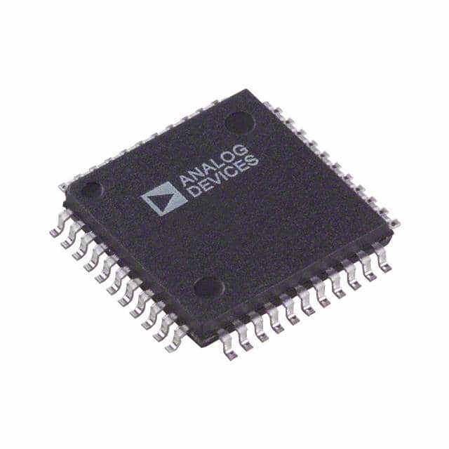
Analog Devices Inc. AD1893JST
- Part No.:
- AD1893JST
- Manufacturer:
- Analog Devices Inc.
- Category:
- Encoders, Decoders, Converters
- Package:
- 44-LQFP
- Datasheet:
-
 AD1893JST.pdf
- Description:
- IC SAMPLE-RATE CONV 16BIT 44LQFP
- Quantity:
- Payment:

- Shipping:

Inventory:53,627
Please send an inquiry. Send us your inquiry, and we will respond immediately.
Product details
Overview
AD1893JST from Analog Devices is a 16-bit stereo asynchronous sample rate converter (ASRC) designed for digital audio interfacing between mismatched sample clocks (e.g., 44.1 kHz CD ↔ 48 kHz DAT). It operates from 2.7–5.5 V, achieves –96 dB THD+N at 1 kHz, supports 8–56 kHz input/output sample rates with 1:2 to 2:1 ratio flexibility, and features on-chip 16 MHz oscillator for crystal-based timing. It targets battery-powered consumer audio recorders and networked multimedia systems.
For engineers reviewing the AD1893JST datasheet, AD1893JST pinout, AD1893JST application, or AD1893JST equivalent, key selection considerations include its automatic sample frequency sensing, jitter rejection up to 10 ns (slow mode), linear-phase FIR filtering with 110 dB stopband attenuation, 700–3000 µs group delay, and LQFP-44 package compatibility with portable audio BOMs.
Technical Context
The AD1893JST implements asynchronous conversion via polyphase FIR filter bank with 65,536 equivalent subfilters, operating at an internal 3.2768 GHz convolution rate and 300 ps time resolution. Its digital servo control loop continuously computes the LR_I/LR_O ratio to drive FIFO read addressing and coefficient ROM selection without external programming.
It supports independent input/output serial interface configurations-including right-justified, left-justified, and word-clock-triggered modes-with programmable bit clock polarity (BKPOL_I/O) and dual-mode settling (SETSLW pin selects ≈200 ms fast or ≈800 ms slow loop response), enabling real-time adaptation to dynamic sample rate changes while maintaining ≤0° interchannel phase deviation.
Key Specifications
| Parameter | Value and Actual Design Meaning |
|---|---|
| Sample Rate Range | 8–56 kHz input and output; enables interoperability across CD (44.1 kHz), DAT (48 kHz), and broadcast (32 kHz) standards. |
| THD+N | –96 dB at 1 kHz full-scale; ensures high-fidelity audio reproduction with minimal harmonic distortion in consumer playback paths. |
| Dynamic Range | 96 dB (20 Hz–20 kHz, –60 dB input); provides wide signal-to-noise margin for low-level audio detail preservation. |
| Jitter Tolerance | ≤10 ns input/output clock jitter (slow mode); rejects timing noise from low-cost oscillators or long PCB traces without degrading THD+N. |
| Filter Performance | 0.01 dB passband ripple, 4.1 kHz transition band, 110 dB stopband attenuation; maintains flat 20 kHz bandwidth even at 44.1 kHz sampling. |
| Power Consumption | 15–20 mA at 3.0 V (typical); supports extended battery life in portable CD-R, DAT, and MD recorders. |
| Group Delay | 700–3000 µs (LR_I = 50 kHz); enables predictable latency budgeting in real-time audio pipelines with FIFO-based buffering. |
Pinout & Package
AD1893JST is housed in a 10 mm × 10 mm LQFP-44 package with exposed thermal pad (ST-44), rated for 0°C to +70°C operation. Pin functions are validated per Analog Devices AD1893 datasheet Rev. A (pages 5–7).
| Pin/Terminal | Circuit Role | Design Meaning |
|---|---|---|
| DATA_I (Pin 43) | Serial input data | MSB-first 4–16-bit two's-complement stereo data; zero-filled LSBs for shorter words; interfaces directly to DSP or AES/EBU receiver outputs. |
| LR_I (Pin 4) | Input left/right clock | Continuous 8–56 kHz clock defining input sample boundaries; used by servo loop to track FSIN for ASRC ratio calculation. |
| SETSLW (Pin 38) | Settle mode control | HI = slow mode (≈800 ms loop settling, >3 Hz jitter rejection); LO = fast mode (≈200 ms, supports varispeed tracking); dynamically switchable. |
| MUTE_O / MUTE_I (Pins 20 / 18) | FIFO error signaling & output muting | MUTE_O asserts HI during FIFO underflow/overflow (128 cycles); tied to MUTE_I to force zero-output mute-prevents pop/click artifacts during transient rate shifts. |
| XTAL_I / XTAL_O (Pins 42 / 40) | Crystal oscillator interface | Drives internal 16 MHz oscillator with external crystal; eliminates need for external clock generator-reduces BOM count and layout complexity. |
Key Features
| Feature | Design Value |
|---|---|
| Automatic sample rate detection | No firmware or register programming required-senses LR_I/LR_O ratio in real time, enabling plug-and-play integration across mixed-audio-source systems. |
| Linear-phase FIR filtering | Preserves phase coherence between stereo channels (0° interchannel deviation), critical for spatial audio imaging in consumer playback devices. |
| Flexible serial interface modes | Independent configuration of input/output justification (right/left/WCLK-triggered) and bit clock polarity via MODE0/1 and BKPOL pins-supports I²S, left-justified, and custom DSP protocols. |
| On-chip oscillator | Reduces external component count by eliminating discrete oscillator; only requires 16 MHz crystal-lowers total system cost and board area in portable designs. |
| Power-down mode | PWRDWN pin reduces current to 0.5–1.0 mA at 3.0 V, enabling rapid sleep/wake cycling in battery-operated recorders without losing state. |
Applications
| CD/DAT Interfacing | Digital Audio Networking |
|---|---|
Use Scenario: Bridging 44.1 kHz CD audio streams to 48 kHz DAT recording hardware in portable consumer devices. IC Role / Device Role / Timing Role: Asynchronous sample rate converter synchronizing independent clock domains without shared master clock or PLL locking. Use Value: Eliminates audible pitch shift and dropouts caused by sample rate mismatch, enabling seamless analog-to-digital transfer with <1 ppm timing error. | Use Scenario: Integrating AES/EBU receivers and transmitters with differing sample clocks in studio-grade digital audio networks. IC Role / Device Role / Timing Role: Digital audio bridge IC performing real-time resampling between asynchronous network nodes using LR_I/LR_O as timing references. Use Value: Maintains bit-perfect audio integrity across clock domains while rejecting jitter from long cable runs-preserving SNR and THD+N specs end-to-end. |
| Computer Multimedia | Portable Audio Recorders |
Use Scenario: Resolving sample rate conflicts between PC sound cards (48 kHz default) and legacy 44.1 kHz audio content libraries. IC Role / Device Role / Timing Role: Standalone ASRC placed between host controller and codec, decoupling software-driven sample rate selection from hardware clock constraints. Use Value: Enables OS-level sample rate switching without hardware reconfiguration-reducing driver complexity and improving user experience in multimedia applications. | Use Scenario: Enabling simultaneous recording from multiple analog sources (mic, line-in) with independent sample rate requirements in handheld MD or DCC recorders. IC Role / Device Role / Timing Role: Low-voltage (2.7–5.5 V), low-power (15–20 mA @ 3 V) ASRC providing battery-efficient sample rate translation in space-constrained portable enclosures. Use Value: Extends operating time by >30% versus 5 V alternatives while maintaining 96 dB dynamic range-critical for all-day field recording. |
Equivalent & Alternatives
The following parts are listed as comparable options for similar asynchronous sample rate conversion applications.
| Alternative Part | Technical Difference | Application Difference | Selection Advice |
|---|---|---|---|
| AK4118VN | 24-bit I²S-only interface; no on-chip oscillator-requires external 24.576 MHz clock; higher THD+N (–90 dB) at 1 kHz. | Targeted at fixed-format professional audio gear with stable master clocks; lacks auto-sensing and flexible justification modes. | Choose AK4118VN only when I²S-native design and external clock infrastructure already exist; not suitable for battery-powered or crystal-only systems. |
| CS8422-CQZ | Includes integrated S/PDIF receiver/transmitter; wider supply range (4.5–5.5 V); no fast/slow settling mode-fixed 500 ms loop response. | Optimized for S/PDIF-centric consumer AV receivers; higher power draw (35 mA @ 5 V) limits portable use. | Prefer CS8422-CQZ when S/PDIF interface and embedded receiver functionality are required; avoid if low-voltage operation or dynamic rate tracking is critical. |
Compared with AK4118VN and CS8422-CQZ, AD1893JST uniquely combines crystal-based self-timing, automatic rate sensing, dual-mode jitter rejection, and 3 V operation-making it the only option qualified for cost-sensitive, battery-powered, multi-standard consumer audio recorders requiring zero-configuration interoperability.
Availability
AD1893JST is available at Aetrix Electronics and suitable for consumer audio recorders, digital audio networking equipment, and computer multimedia systems requiring stable component supply, long-term lifecycle support, and RoHS-compliant packaging.
Supply support for AD1893JST includes scheduled delivery planning, volume procurement assistance, BOM continuity management, traceable sourcing, and lifecycle availability coordination for OEM customers, industrial embedded developers, connected-device designers, and electronics production programs.
Manufacturer
Analog Devices is a U.S.-based semiconductor company specializing in high-performance analog, mixed-signal, and digital signal processing technologies for precision instrumentation, communications, and industrial applications.
The AD1893JST belongs to the SamplePort® family of asynchronous sample rate converters, engineered specifically for low-cost, low-power digital audio bridging in portable and consumer electronics where battery life, board space, and multi-standard compatibility are critical.
FAQ
What is the primary function of the AD1893JST in a digital audio system?
The AD1893JST serves as a fully digital stereo asynchronous sample rate converter that bridges mismatched input and output sample clocks-such as 44.1 kHz CD audio and 48 kHz DAT streams-without requiring shared timing references or firmware configuration. Its core function is to maintain audio fidelity during real-time resampling by dynamically computing the LR_I/LR_O ratio and applying linear-phase FIR filtering. The AD1893JST achieves this with –96 dB THD+N and 96 dB dynamic range while operating from a single 3 V supply.
Does the AD1893JST require external programming to handle different sample rates like 32 kHz, 44.1 kHz, or 48 kHz?
No, the AD1893JST does not require external programming or register writes to handle 32 kHz, 44.1 kHz, or 48 kHz sample rates. It automatically senses the relationship between the input (LR_I) and output (LR_O) sample clocks and adapts its internal interpolation/decimation ratio accordingly. This auto-sensing capability covers the full 8–56 kHz range and supports dynamic rate changes-even mid-stream-making the AD1893JST ideal for multi-standard consumer audio devices where manual configuration is impractical.
How does the SETSLW pin affect the performance of the AD1893JST?
The SETSLW pin configures the AD1893JST's digital servo control loop settling time: HI selects slow mode (≈800 ms settling, >3 Hz jitter rejection), optimizing for maximum signal quality in static-rate applications; LO selects fast mode (≈200 ms settling), enabling rapid tracking of real-time sample rate variations at the cost of narrowband noise modulation. This pin is asynchronous and can be changed dynamically-allowing the AD1893JST to adapt its behavior based on operational context without resetting or reinitialization.
Can the AD1893JST operate from a 3.0 V supply, and what is its typical current draw at that voltage?
Yes, the AD1893JST is fully specified for operation from 2.7 V to 5.5 V, with guaranteed performance at 3.0 V. At 3.0 V supply and typical conditions (FSIN = 48 kHz, FSOUT = 44.1 kHz), its operational current is 15–20 mA, and power-down current drops to 0.5–1.0 mA. This low-voltage, low-power profile makes the AD1893JST especially suitable for battery-powered portable audio recorders where energy efficiency directly impacts runtime.
What package type and pin count does the AD1893JST use, and is it compatible with standard PCB assembly processes?
The AD1893JST uses a 44-pin LQFP (ST-44) package measuring 10 mm × 10 mm with an exposed thermal pad, compliant with JEDEC MS-026. It is compatible with standard surface-mount reflow processes including lead-free soldering (up to 300°C for 10 seconds). The pinout is fully documented in the Analog Devices AD1893 datasheet Rev. A, and the package supports automated optical inspection and X-ray verification-ensuring high-yield manufacturing for consumer audio production lines.
AD1893JST Specifications
- Product attributes
- Attribute value
- Manufacturer:
- Analog Devices Inc.
- Series:
- SamplePort™
- Package/Case:
- 44-LQFP
- Packaging:
- Bag
- Product Status:
- Obsolete
- Type:
- Sample Rate Converter
- Applications:
- Multimedia
- Voltage - Supply, Analog:
- -
- Voltage - Supply, Digital:
- 2.7V ~ 5.5V
- Grade:
- -
- Qualification:
- -
- Mounting Type:
- Surface Mount
- Supplier Device Package:
- 44-LQFP (10x10)
AD1893JST FAQ
1.How can I place an order for AD1893JST through Aetrix?
Please submit a Request for Quotation (RFQ) for AD1893JST on Aetrix. Our sales agent will provide a competitive quotation and guide you through the order confirmation once you accept the terms.
2.Are the price and stock information for AD1893JST reliable?
The price and inventory of AD1893JST are updated periodically and may fluctuate due to market conditions. Stock and pricing data are typically refreshed every 24 hours. Quotation validity for AD1893JST is usually 5 days.
3.What payment methods are accepted for AD1893JST?
We accept Wire Transfer, PayPal, Credit Card, Western Union, MoneyGram, and Escrow for AD1893JST transactions.
Note: Certain payment methods may incur a processing fee.
4.How is shipping managed for AD1893JST?
AD1893JST orders can be shipped via leading logistics carriers, including DHL, UPS, FedEx, TNT, or Registered Mail.
Once your AD1893JST order is processed, you will receive an email with the shipment details and tracking number.
Note: Tracking information may take up to 24 hours to appear. Express delivery typically takes 3–5 business days.
5.How can I obtain technical support or documentation for AD1893JST?
For technical support, including AD1893JST datasheets, pinout diagrams, or application guidance, please contact our engineering support team. They can provide detailed documentation and assistance for your AD1893JST requirements.
6.How does Aetrix verify that AD1893JST is sourced from the original manufacturer or authorized distributors?
All AD1893JST products on Aetrix are procured from qualified distributors and authorized channels. Our dedicated quality assurance team conducts strict verification, including traceability checks and, if necessary, third-party testing. This ensures that AD1893JST meets industry standards.
7.What is the process for return or replacement of AD1893JST?
All AD1893JST units undergo pre-shipment inspection (PSI). If there is an issue with AD1893JST, returns or replacements are accepted under the following conditions:
1.Quantity discrepancies, incorrect items, or visible external defects (such as breakage or corrosion), acknowledged by Aetrix.
2.The issue is reported within 90 days of delivery.
3.The AD1893JST part is unused and in its original packaging.
Return procedure for AD1893JST:
1.Submit a request within 90 days.
2.Obtain a Return Material Authorization (RMA) from Aetrix.
AD1893JST Tags

-
MCP2120T-I/SL
Microchip Technology

-
LICAL-ENC-MS001
TE Connectivity Linx
-
TW9990AT-NA1-GR
Renesas Electronics Corporation
-
TVP5151IPBSR
Texas Instruments
-
TVP5150AM1IPBSR
Texas Instruments
-
LICAL-DEC-MS001-T
TE Connectivity Linx
-
ADV7391BCPZ
Analog Devices Inc.
-
ADV7393BCPZ-REEL
Analog Devices Inc.
-
ADV7393BCPZ
Analog Devices Inc.
-
ADV7391WBCPZ
Analog Devices Inc.
-
ADV7181DBCPZ
Analog Devices Inc.

-
ADV7181CBSTZ-REEL
Analog Devices Inc.
Tech Hub

A practical engineering guide to 3.3V and 5V logic compatibility, input thresholds, resistor dividers, translator ICs, MOSFET level shifting, I2C pull-ups, timing limits and power-sequencing risks.

The 74HC595 uses push-pull logic outputs, while the TPIC6B595 uses 50 V open-drain DMOS sinks for higher-power loads. This guide compares timing, current limits, 3.3 V interfacing, load wiring, thermal…

The 74HC595 converts serial data into eight stable parallel outputs. This guide covers pin functions, shift and storage timing, OE and MR behavior, drive-current limits, cascading, voltage compatibilit…

A technical comparison of level-sensitive latches and edge-triggered flip-flops, covering timing windows, setup and hold limits, master–slave operation, time borrowing, race-through, HDL inference and…

A D latch stores one bit while Enable controls when data can pass. This reference covers gate-level operation, truth tables, transparency, setup and hold timing, LE versus OE, common ICs and practical …

An SR latch stores one bit through cross-coupled feedback. This engineering reference covers NOR and NAND implementations, truth tables, forbidden-state recovery, gated operation, switch debouncing, fa…

Latch circuits retain one bit through feedback. This technical reference covers SR and D latches, truth tables, transparency, timing limits, latch-versus-flip-flop behavior, applications and common log…

An engineering guide to LED driver operation, constant-current and constant-voltage outputs, linear and switching topologies, dimming, IC selection, calculations, replacement compatibility, and fault c…

Operational amplifier guide covering op amp basics, feedback, ideal vs real op amps, common configurations, buffer circuits, offset, bias current, gain-bandwidth, slew rate, rail-to-rail limits and sel…

Jumper cables guide covering safe connection order, red and black clamp placement, final ground connection, cable gauge, length, clamp quality, copper vs CCA cables, jump starter comparison and battery…


