
 My Inquiry
 My Account


Analog Devices Inc. AD261BND-2
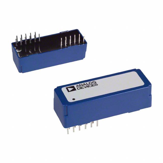
- Part No.:
- AD261BND-2
- Manufacturer:
- Analog Devices Inc.
- Category:
- Digital Isolators
- Package:
- 22-DIP Module
- Datasheet:
-
 AD261BND-2.pdf
- Description:
- DGTL ISO 3500VRMS 5CH GP 22DIP
- Quantity:
- Payment:

- Shipping:

Inventory:4,569
Please send an inquiry. Send us your inquiry, and we will respond immediately.
Product details
Overview
AD261BND-2 from Analog Devices is a high-speed logic isolator with 2 input / 3 output unidirectional channel configuration, 3.5 kVrms isolation rating, 20 MHz minimum signal bandwidth, and 14 ns typical propagation delay. It replaces up to five optocouplers in industrial I/O modules requiring precise PWM signal isolation and field/system side decoupling.
For engineers reviewing the AD261BND-2 datasheet, AD261BND-2 pinout, AD261BND-2 application, or AD261BND-2 equivalent, this page delivers verified specifications, exact pin functions for the ND-22A DIP-22 package, real-world use cases in PLC analog I/O and motor drive controls, and two validated alternative isolators with documented functional trade-offs.
Technical Context
The AD261BND-2 implements five isolated HCMOS-compatible logic channels using capacitive isolation with set-hi/set-lo data encoding across a 3.5 kVrms tested barrier. Each channel features a Schmitt-trigger input (2.0–4.2 V threshold range) and three-state output controlled by ENABLESYS/ENABLEFLD pins.
It supports continuous background update (every ~5 µs) to guarantee valid output states within 12 µs after power-up or fault recovery, and maintains ±1 ns edge symmetry error between rising/falling transitions - critical for accurate time-based signal isolation such as PWM and encoder timing.
Key Specifications
| Parameter | Value and Actual Design Meaning |
|---|---|
| Isolation Rating | 3.5 kVrms production-tested (VDE/IEC950/EN60950 certified); enables safe interface between 750 V mains-referenced field circuits and low-voltage system logic. |
| Signal Bandwidth | 20 MHz min; supports reliable transmission of fast digital control signals including 25 ns minimum pulsewidths and high-frequency bus protocols. |
| Propagation Delay | 14 ns typ (max 25 ns); ensures tight timing alignment across isolated domains for synchronous control loops and real-time feedback systems. |
| CMV Transient Immunity | 10 kV/µs min; prevents false triggering during high-dV/dt events common in IGBT motor drives and industrial switching environments. |
| I/O Configuration | 2 inputs (S0–S1), 3 outputs (F0–F2); fixed directionality per pin per model - no bidirectional operation or software reconfiguration. |
| Supply Voltage Range | 4.0–5.75 V dc per side (system & field); accommodates brown-out conditions while maintaining full specification compliance down to –25°C. |
| Power Dissipation | 18 mA total at 10 MHz (both sides); enables predictable thermal design in dense PLC backplane layouts without forced cooling. |
Pinout & Package
AD261BND-2 uses the 22-pin plastic DIP package (ND-22A) with 18 mm creepage spacing between system and field sides, supporting CSA/IS and IEC 750 V mains isolation requirements. Pin 1 is marked with a notch; pins 9–14 are not present.
| Pin/Terminal | Circuit Role | Design Meaning |
|---|---|---|
| 1–2 (S0, S1) | System-side Inputs | Digital transmit lines from microcontroller or system logic; configured as inputs only for AD261BND-2 per Table I. |
| 3–5 (S2–S4) | No-connect (NC) | Physically present but unused; must be tied high/low per datasheet guidance - not floating. |
| 6 (ENABLESYS) | System Output Enable | Active-low control: pulls all system-side outputs (none on AD261BND-2) into high-impedance state; used for multiplexing multiple AD261s. |
| 7 (+5 VdcSYS) | System Power Supply | +5 V supply for system-side circuitry; requires local 0.01 µF bypass capacitor per datasheet recommendation. |
| 8 (5 V RTNSYS) | System Ground Reference | Return path for system-side supply; separate from field ground to maintain isolation integrity. |
| 15 (5 V RTNFLD) | Field Ground Reference | Return path for field-side supply; galvanically isolated from 5 V RTNSYS. |
| 16 (+5 VdcFLD) | Field Power Supply | +5 V supply for field-side receivers; independent regulation required to avoid coupling noise across barrier. |
| 17 (ENABLEFLD) | Field Output Enable | Active-low control: places F0–F2 outputs in high-Z state; allows presetting logic levels via pull-ups at power-up. |
| 18–20 (F0–F2) | Field-side Outputs | Digital receive lines driving field I/O (e.g., ADC/DAC control, relay drivers); unidirectional and non-inverting. |
| 21–22 (F3–F4) | No-connect (NC) | Physically present but unused; must be tied high/low - not left floating per datasheet warning. |
Key Features
| Feature | Design Value |
|---|---|
| Five-channel capacitive isolation | Replaces five discrete optocouplers with matched timing, reduced board area, and no LED aging or CTR degradation. |
| Continuous background update | Guarantees valid output state ≤12 µs after power-up or fault - eliminates need for external reset sequencing in safety-critical I/O. |
| ±1 ns edge symmetry error | Maintains precise duty cycle fidelity for PWM signals used in motor phase control and precision DAC timing. |
| 10 kV/µs CMV immunity | Withstands fast transients from IGBT switching without latch-up or false output toggling - critical for drive interface reliability. |
| Pin-compatible family | Shares identical ND-22A footprint and enable/power pin locations across all six AD261 variants - simplifies BOM consolidation and layout reuse. |
Applications
| PLC Analog Input Card | IGBT Motor Drive Interface |
|---|---|
|
Use Scenario: Isolating microcontroller GPIOs from 4–20 mA current loop transmitters and ADC reference circuits in modular PLC backplanes. IC Role / Device Role / Timing Role: AD261BND-2 provides 2 system-side control inputs (e.g., channel enable, gain select) and 3 field-side status outputs (e.g., overcurrent flag, ready signal, fault latch). Use Value: Eliminates ground loop errors and protects system-side logic from field-side surge events while preserving sub-25 ns timing resolution for synchronized sampling. |
Use Scenario: Interfacing MCU PWM outputs and status feedback between gate driver ICs and main controller in variable-frequency AC drives. IC Role / Device Role / Timing Role: AD261BND-2 routes two PWM enable/control signals from system side and returns three isolated status lines (UVLO, DESAT, READY) from field-side gate drivers. Use Value: Enables safe, high-fidelity PWM transmission with <14 ns delay and ±1 ns edge matching - essential for phase-aligned multi-phase inverter control. |
| Industrial Data Acquisition Hub | High-Speed Digital I/O Module |
|
Use Scenario: Centralized isolation for sensor excitation control and diagnostic feedback in multi-channel DAQ systems with mixed voltage domains. IC Role / Device Role / Timing Role: AD261BND-2 delivers two system-initiated commands (e.g., calibration start, range select) and receives three field-side responses (e.g., sensor OK, temp alert, self-test pass). Use Value: Provides 3.5 kVrms isolation and 10 kV/µs transient rejection to prevent measurement corruption from EMI-rich factory floor environments. |
Use Scenario: Modular digital I/O card supporting configurable input/output mapping in automation controllers with hot-swap capability. IC Role / Device Role / Timing Role: AD261BND-2 serves as a fixed 2-in/3-out isolator block within a larger I/O ASIC or FPGA subsystem, enabling flexible firmware-defined channel assignment. Use Value: Delivers deterministic 20 MHz bandwidth and three-state enable for seamless bus sharing among multiple AD261BND-2 units on shared field-side traces. |
Equivalent & Alternatives
The following parts are listed as comparable options for similar high-speed logic isolation applications.
| Alternative Part | Technical Difference | Application Difference | Selection Advice |
|---|---|---|---|
| Si8623BD-B-IS | 2-channel, 25 Mbps (≈25 MHz), 3.75 kVrms, SOIC-16; no enable pins, no continuous update feature. | Lacks three-state enable and background refresh - unsuitable where output state retention during enable cycling is required. | Choose when compact size and higher isolation voltage outweigh need for output enable and guaranteed post-reset validity. |
| ISO6721DR | 2-channel, 50 Mbps (≈50 MHz), 5 kVrms, SOIC-8; single supply (3.3–5.5 V), no dedicated field/system enable pins. | Requires level-shifting for asymmetric supply configurations; lacks dual-enable architecture for independent field/system bus control. | Prefer when maximum speed and smallest footprint are primary, and system-level enable management can replace per-side EN pins. |
Compared with Si8623BD-B-IS and ISO6721DR, the AD261BND-2 uniquely combines dual independent enable pins, guaranteed 12 µs output validity after power-up, and fixed 2-in/3-out topology in a through-hole DIP package - making it optimal for legacy industrial designs requiring robust, maintenance-friendly isolation with deterministic timing behavior.
Availability
AD261BND-2 is available at Aetrix Electronics and suitable for PLC analog input cards, IGBT motor drive interfaces, and industrial data acquisition hubs requiring stable component supply, long-term lifecycle support, and traceable sourcing for safety-critical deployments.
Supply support for AD261BND-2 includes scheduled delivery planning, volume procurement assistance, BOM continuity management, traceable sourcing, and lifecycle availability coordination for OEM customers, industrial embedded developers, connected-device designers, and electronics production programs.
Manufacturer
Analog Devices is a global leader in high-performance analog, mixed-signal, and digital signal processing semiconductors, serving industrial, automotive, communications, and healthcare markets since 1965.
The AD261 product line was designed specifically for high-reliability industrial digital isolation - delivering optocoupler replacement with superior speed, timing accuracy, and transient immunity in harsh electromagnetic environments.
FAQ
What is the isolation voltage rating of the AD261BND-2?
The AD261BND-2 is rated for 3.5 kVrms isolation test voltage and has an operating isolation voltage of 1.25 kVrms. This rating is 100% production-tested per Analog Devices' standard method and supports UL1950, IEC950, and EN60950 certification. The AD261BND-2 achieves this with >18 mm creepage distance in its ND-22A package, enabling safe operation in 750 V mains-referenced field circuits.
How does the AD261BND-2 handle power-up and fault recovery?
The AD261BND-2 guarantees valid output states within 12 µs after power-up or fault recovery due to its continuous background update circuit, which interrogates inputs every ~5 µs. Unlike optocouplers or basic digital isolators, the AD261BND-2 does not require external reset signals - its internal logic ensures F0–F2 reflect true S0–S1 states without delay or ambiguity, critical for fail-safe I/O in industrial controllers.
Can unused pins on the AD261BND-2 be left floating?
No - unused pins on the AD261BND-2 (S2–S4 and F3–F4) must be tied either high or low and never left floating. The datasheet explicitly warns that floating inputs can cause unpredictable behavior, increased power consumption, or susceptibility to noise. This requirement applies regardless of whether the pin is physically present (pins 1–5 and 18–22) or absent (pins 9–14).
What is the function of ENABLESYS and ENABLEFLD on the AD261BND-2?
ENABLESYS (pin 6) and ENABLEFLD (pin 17) are active-low enable pins that place all outputs on their respective sides into high-impedance three-state mode. For AD261BND-2, ENABLEFLD controls F0–F2 outputs, allowing presetting of logic levels via pull-up/down resistors at power-up; ENABLESYS is reserved for future expansion or multiplexing but has no effect on outputs in this variant.
Does the AD261BND-2 support bidirectional communication?
No - the AD261BND-2 implements strictly unidirectional logic channels: S0 and S1 are inputs only, F0–F2 are outputs only. Directionality is hardwired per model; there is no software or hardware mechanism to reverse signal flow. For bidirectional isolation, multiple AD261 devices or alternate solutions like the ADuM1201 would be required.
AD261BND-2 Specifications
- Product attributes
- Attribute value
- Manufacturer:
- Analog Devices Inc.
- Series:
- IsoLogic™
- Package/Case:
- 22-DIP Module
- Packaging:
- Bulk
- Product Status:
- Obsolete
- Technology:
- Magnetic Coupling
- Type:
- General Purpose
- Isolated Power:
- No
- Number of Channels:
- 5
- Inputs - Side 1/Side 2:
- 2/3
- Channel Type:
- Unidirectional
- Voltage - Isolation:
- 3500Vrms
- Common Mode Transient Immunity (Min):
- 10kV/µs
- Data Rate:
- -
- Propagation Delay tpLH / tpHL (Max):
- 25ns, 25ns
- Pulse Width Distortion (Max):
- -
- Rise / Fall Time (Typ):
- -
- Voltage - Supply:
- 4V ~ 5.75V
- Grade:
- -
- Qualification:
- -
- Operating Temperature:
- -25°C ~ 85°C
- Mounting Type:
- Through Hole
- Supplier Device Package:
- 22-PDIP
AD261BND-2 FAQ
1.How can I place an order for AD261BND-2 through Aetrix?
Please submit a Request for Quotation (RFQ) for AD261BND-2 on Aetrix. Our sales agent will provide a competitive quotation and guide you through the order confirmation once you accept the terms.
2.Are the price and stock information for AD261BND-2 reliable?
The price and inventory of AD261BND-2 are updated periodically and may fluctuate due to market conditions. Stock and pricing data are typically refreshed every 24 hours. Quotation validity for AD261BND-2 is usually 5 days.
3.What payment methods are accepted for AD261BND-2?
We accept Wire Transfer, PayPal, Credit Card, Western Union, MoneyGram, and Escrow for AD261BND-2 transactions.
Note: Certain payment methods may incur a processing fee.
4.How is shipping managed for AD261BND-2?
AD261BND-2 orders can be shipped via leading logistics carriers, including DHL, UPS, FedEx, TNT, or Registered Mail.
Once your AD261BND-2 order is processed, you will receive an email with the shipment details and tracking number.
Note: Tracking information may take up to 24 hours to appear. Express delivery typically takes 3–5 business days.
5.How can I obtain technical support or documentation for AD261BND-2?
For technical support, including AD261BND-2 datasheets, pinout diagrams, or application guidance, please contact our engineering support team. They can provide detailed documentation and assistance for your AD261BND-2 requirements.
6.How does Aetrix verify that AD261BND-2 is sourced from the original manufacturer or authorized distributors?
All AD261BND-2 products on Aetrix are procured from qualified distributors and authorized channels. Our dedicated quality assurance team conducts strict verification, including traceability checks and, if necessary, third-party testing. This ensures that AD261BND-2 meets industry standards.
7.What is the process for return or replacement of AD261BND-2?
All AD261BND-2 units undergo pre-shipment inspection (PSI). If there is an issue with AD261BND-2, returns or replacements are accepted under the following conditions:
1.Quantity discrepancies, incorrect items, or visible external defects (such as breakage or corrosion), acknowledged by Aetrix.
2.The issue is reported within 90 days of delivery.
3.The AD261BND-2 part is unused and in its original packaging.
Return procedure for AD261BND-2:
1.Submit a request within 90 days.
2.Obtain a Return Material Authorization (RMA) from Aetrix.
AD261BND-2 Tags

-
ISO1212DBQR
Texas Instruments
-
ISO6721BDR
Texas Instruments
-
SI8710AC-B-ISR
Skyworks Solutions Inc.
-
ISO7720FDR
Texas Instruments
-
ISO7721DR
Texas Instruments
-
ISO7721FDR
Texas Instruments
-
SI8710CC-B-ISR
Skyworks Solutions Inc.
-
ISO6741FQDWRQ1
Texas Instruments

-
ISO7721DWVR
Texas Instruments
-
ISO7762FDBQR
Texas Instruments

-
ISO7741DWR
Texas Instruments
-
ISO7741FDWR
Texas Instruments
Tech Hub

A practical engineering guide to 3.3V and 5V logic compatibility, input thresholds, resistor dividers, translator ICs, MOSFET level shifting, I2C pull-ups, timing limits and power-sequencing risks.

The 74HC595 uses push-pull logic outputs, while the TPIC6B595 uses 50 V open-drain DMOS sinks for higher-power loads. This guide compares timing, current limits, 3.3 V interfacing, load wiring, thermal…

The 74HC595 converts serial data into eight stable parallel outputs. This guide covers pin functions, shift and storage timing, OE and MR behavior, drive-current limits, cascading, voltage compatibilit…

A technical comparison of level-sensitive latches and edge-triggered flip-flops, covering timing windows, setup and hold limits, master–slave operation, time borrowing, race-through, HDL inference and…

A D latch stores one bit while Enable controls when data can pass. This reference covers gate-level operation, truth tables, transparency, setup and hold timing, LE versus OE, common ICs and practical …

An SR latch stores one bit through cross-coupled feedback. This engineering reference covers NOR and NAND implementations, truth tables, forbidden-state recovery, gated operation, switch debouncing, fa…

Latch circuits retain one bit through feedback. This technical reference covers SR and D latches, truth tables, transparency, timing limits, latch-versus-flip-flop behavior, applications and common log…

An engineering guide to LED driver operation, constant-current and constant-voltage outputs, linear and switching topologies, dimming, IC selection, calculations, replacement compatibility, and fault c…

Operational amplifier guide covering op amp basics, feedback, ideal vs real op amps, common configurations, buffer circuits, offset, bias current, gain-bandwidth, slew rate, rail-to-rail limits and sel…

Jumper cables guide covering safe connection order, red and black clamp placement, final ground connection, cable gauge, length, clamp quality, copper vs CCA cables, jump starter comparison and battery…


