
 My Inquiry
 My Account


Analog Devices Inc. AD2S99AP
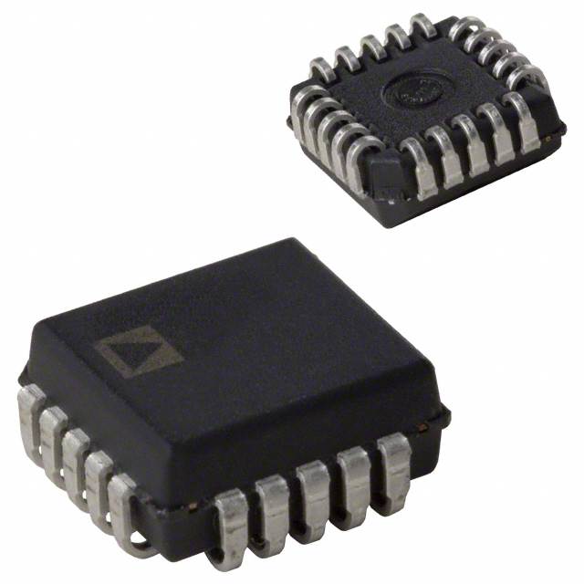
- Part No.:
- AD2S99AP
- Manufacturer:
- Analog Devices Inc.
- Category:
- Programmable Timers and Oscillators
- Package:
- 20-LCC (J-Lead)
- Datasheet:
-
 AD2S99AP.pdf
- Description:
- IC OSC SINUSOIDAL PROG 20-PLCC
- Quantity:
- Payment:

- Shipping:

Inventory:2,608
Please send an inquiry. Send us your inquiry, and we will respond immediately.
Product details
Overview
AD2S99AP from Analog Devices is a programmable sinusoidal oscillator IC designed to provide precision excitation and synchronous reference generation for resolver, synchro, LVDT, and RVDT transducers. It delivers 2–20 kHz programmable excitation (±10% accuracy over –40°C to +85°C), ±3 Vp-p square-wave SYNREF output phase-locked to SIN/COS inputs, and integrated loss-of-signal (LOS) detection. It serves as the excitation source and dynamic phase compensation engine in high-accuracy angular position sensing systems.
For engineers reviewing the AD2S99AP datasheet, AD2S99AP pinout, AD2S99AP application, or AD2S99AP equivalent, key selection considerations include its 20-pin PLCC package, dual EXC outputs with 180° phase relationship, FBIAS-based intermediate frequency tuning, LOS open-drain logic indicator, and compatibility with AD2S80A/AD2S82A/AD2S90 R/D converters.
Technical Context
The AD2S99AP implements a closed-loop phase detection architecture that dynamically locks its SYNREF output to the phase of incoming SIN and COS feedback signals-enabling real-time compensation for temperature- and cable-induced phase shifts in resolver secondary windings. Its internal sine wave generator drives differential EXC/EXC outputs (2 Vrms, low THD) while supporting four factory-selectable frequencies via SEL1/SEL2 pins.
Frequency programming is achieved through digital pin strapping (2/5/10/20 kHz) or analog fine-tuning via FBIAS resistor-to-VDD connection. The LOS circuit monitors both SIN and COS amplitudes against a 0.6 Vrms threshold and asserts an open-drain high signal when both fall below it-providing fail-safe transducer disconnection detection without external components.
Key Specifications
| Parameter | Value and Actual Design Meaning |
|---|---|
| Excitation Frequency Range | 2 kHz, 5 kHz, 10 kHz, or 20 kHz (pin-selectable); intermediate values via FBIAS resistor |
| Excitation Output Amplitude | 2 Vrms across 500 Ω load-sufficient to drive typical resolver primaries without buffering |
| SYNREF Output | ±3 Vp-p square wave, phase-coherent with SIN/COS inputs-used as zero-crossing reference for R/D converters |
| Loss-of-Signal Threshold | 0.6 Vrms (typical) on both SIN and COS-triggers open-drain LOS high alert for system-level fault handling |
| Operating Temperature | –40°C to +85°C-validated for industrial and avionics-grade motion control environments |
| Supply Voltage | ±4.75 V to ±5.25 V-supports standard dual-rail analog power domains with 15 mA total quiescent current |
| Package | 20-pin PLCC (P-20A)-surface-mount compatible with automated assembly and thermal performance up to 85°C ambient |
Pinout & Package
AD2S99AP is housed in a 20-pin Plastic Leaded Chip Carrier (PLCC, package code P-20A) with gull-wing leads. Pins 19 and 20 are internally connected VSS terminals; pins 6 (DGND) and 16 (AGND) must be externally shorted at the device footprint. NC pins (3, 4, 9, 13, 14, 15) are not bonded and must remain unconnected.
| Pin/Terminal | Circuit Role | Design Meaning |
|---|---|---|
| 1 (SEL2), 2 (SEL1) | Frequency select inputs | Digital control lines determining nominal excitation frequency (2/5/10/20 kHz); must be set before power-up |
| 5 (SIN), 7 (COS) | Transducer feedback inputs | Accept 2 Vrms ±10% resolver secondary outputs for phase lock and LOS monitoring |
| 10 (SYNREF) | Synchronous reference output | Phase-locked ±3 Vp-p square wave used as REF input for AD2S80A/AD2S82A/AD2S90 R/D converters |
| 11 (LOS) | Loss-of-signal indicator | Open-drain output pulled high when both SIN and COS fall below 0.6 Vrms; requires external 50 kΩ pull-up to VDD |
| 17 (EXC), 18 (EXC) | Differential excitation outputs | 180° phase-opposed 2 Vrms sine waves driving resolver primary winding; each capable of 8 mA rms into 500 Ω |
| 12 (VDD), 19 & 20 (VSS) | Power supply terminals | ±5 V dual supply rails; VSS pins must be tied together and decoupled locally with 4.7 µF + 0.1 µF capacitors |
| 16 (AGND), 6 (DGND) | Analog/digital ground | Must be joined at a single point near the device to minimize ground loop noise in precision analog feedback paths |
Key Features
| Feature | Design Value |
|---|---|
| Dynamic phase compensation | Real-time SYNREF phase lock to SIN/COS eliminates need for fixed-phase-shift networks in resolver interfaces |
| Programmable excitation frequency | Four discrete frequencies (2/5/10/20 kHz) plus resistor-tunable intermediate values-enables optimization for transducer bandwidth and EMI |
| Integrated loss-of-signal detection | Single-pin LOS output alerts host controller of open-circuit resolver windings-no external comparators or logic required |
| Dual EXC outputs with 180° phase relationship | Directly drives center-tapped resolver primaries without external inversion or transformer coupling |
| Low THD excitation | –25 dB total harmonic distortion ensures clean fundamental excitation-minimizing position error from harmonic content |
Applications
| Resolver-Based Motor Control | Avionics Flight Surface Position Sensing |
|---|---|
Use Scenario: High-reliability servo motor feedback in electric actuation systems where absolute angular position must be maintained under vibration and temperature cycling. IC Role / Device Role / Timing Role: AD2S99AP generates excitation for the resolver and provides phase-compensated SYNREF to an AD2S82A R/D converter-ensuring <0.5° linearity error across –40°C to +85°C. Use Value: Eliminates manual phase trim and reduces BOM count by integrating excitation, reference, and fault detection in one 20-pin PLCC. |
Use Scenario: Redundant position feedback for aircraft ailerons and rudders, requiring fail-operational behavior and deterministic fault reporting. IC Role / Device Role / Timing Role: AD2S99AP supplies synchronized excitation and reference to dual-channel R/D converters while asserting LOS during resolver disconnect-enabling immediate channel isolation per DO-160E Section 22. Use Value: Open-drain LOS output interfaces directly with flight control computer GPIO, enabling autonomous fault response without software polling. |
| Industrial Hydraulic Valve Position Monitoring | Test Equipment Rotary Encoder Calibration |
Use Scenario: Closed-loop control of proportional hydraulic valves in mobile machinery exposed to wide ambient temperature swings and EMI. IC Role / Device Role / Timing Role: AD2S99AP drives synchro transducers with 5 kHz excitation and feeds phase-stable SYNREF to AD2S90-maintaining <12-bit resolution despite 100 m cable runs. Use Value: Dynamic phase lock compensates for cable capacitance-induced delay, removing need for custom phase-lead networks per installation. |
Use Scenario: Metrology-grade calibration of high-precision rotary encoders using resolver standards traceable to NIST. IC Role / Device Role / Timing Role: AD2S99AP operates at 10 kHz with FBIAS tuning to match reference resolver's optimal frequency-feeding AD2S83 R/D converter with sub-arcminute accuracy. Use Value: Programmable frequency and amplitude stability (±3% @ 25°C) enable repeatable, low-drift measurements across calibration batches. |
Equivalent & Alternatives
The following parts are listed as comparable options for similar programmable transducer excitation applications.
| Alternative Part | Technical Difference | Application Difference | Selection Advice |
|---|---|---|---|
| AD2S99BP | Same functionality and pinout; tighter frequency accuracy (±5% @ +25°C vs. ±10% for AP grade) | Preferred for lab-grade metrology or temperature-stable environments where initial calibration drift must be minimized | Select AD2S99BP when ±5% frequency tolerance at 25°C is required; otherwise AD2S99AP meets industrial motion control needs at lower cost |
| AD2S1210 | Integrated R/D converter (10–16 bit) with built-in excitation-no external SYNREF needed; larger 48-lead LQFP package | Replaces entire AD2S99 + AD2S82A combo; suited for space-constrained designs needing digital angle output | Choose AD2S1210 only if system architecture allows direct SPI angle data-AD2S99AP remains optimal when legacy analog R/D converters (e.g., AD2S82A) are already deployed |
Compared with AD2S99BP, the AD2S99AP trades initial frequency accuracy for cost efficiency in volume industrial applications; compared with AD2S1210, it preserves analog interface flexibility and simplifies upgrade paths for existing resolver signal chains.
Availability
AD2S99AP is available at Aetrix Electronics and suitable for resolver-based motor control, avionics position sensing, and industrial hydraulic valve monitoring requiring stable component supply across extended temperature ranges and long production lifecycles.
Supply support for AD2S99AP includes scheduled delivery planning, volume procurement assistance, BOM continuity management, traceable sourcing, and lifecycle availability coordination for OEM customers, industrial embedded developers, connected-device designers, and electronics production programs.
Manufacturer
Analog Devices, Inc. is a global semiconductor leader specializing in high-performance analog, mixed-signal, and digital signal processing technologies for precision measurement and control.
The AD2S99AP belongs to Analog Devices' resolver interface product line, engineered specifically to simplify high-accuracy angular position feedback in safety-critical motion systems by integrating excitation, phase compensation, and fault detection.
FAQ
What is the function of the FBIAS pin on the AD2S99AP?
The FBIAS pin on the AD2S99AP enables fine-tuning of the excitation frequency beyond the four factory-set values (2/5/10/20 kHz). By connecting a resistor from FBIAS to VDD, users can achieve intermediate frequencies-e.g., 8 kHz is obtained by setting SEL1/GND and SEL2/VSS (10 kHz base) and adding a 6 kΩ resistor. This feature allows optimization for specific transducer resonance or EMI requirements without changing the AD2S99AP hardware layout.
How does the AD2S99AP implement dynamic phase compensation?
The AD2S99AP implements dynamic phase compensation by continuously comparing the phase of incoming SIN and COS signals from the transducer and adjusting its SYNREF output to maintain zero phase error. This closed-loop operation compensates for temperature-dependent phase shifts in resolver windings and cabling delays-eliminating the need for fixed external phase-lead networks and ensuring consistent accuracy across –40°C to +85°C operating range in the AD2S99AP.
Can the AD2S99AP drive a resolver directly without external amplification?
Yes, the AD2S99AP can drive typical resolvers directly: its EXC/EXC outputs deliver 2 Vrms into a 500 Ω load with 8 mA rms current capability. For low-impedance resolvers (<200 Ω) or long cable runs, an external buffer (e.g., OP279) is recommended-but the AD2S99AP's native drive strength suffices for most industrial and aerospace resolvers without added components.
What is the purpose of the LOS output on the AD2S99AP?
The LOS (Loss-of-Signal) output on the AD2S99AP is an open-drain pin that pulls high when both SIN and COS input amplitudes fall below 0.6 Vrms, indicating transducer disconnection or failure. It requires a 50 kΩ pull-up to VDD and provides immediate hardware-level fault signaling-enabling safety controllers to initiate shutdown or redundancy switchover without software intervention in critical AD2S99AP-based systems.
Which R/D converters are explicitly compatible with the AD2S99AP's SYNREF output?
The AD2S99AP's SYNREF output is explicitly designed to interface with Analog Devices' AD2S80A, AD2S82A, AD2S83, and AD2S90 resolver-to-digital converters. The ±3 Vp-p square wave is phase-coherent with SIN/COS inputs and matches the REF input requirements of these devices-though for AD2S90, a 0.1 µF AC-coupling capacitor and 100 kΩ GND resistor are required per the AD2S99AP datasheet Figure 3.
AD2S99AP Specifications
- Product attributes
- Attribute value
- Manufacturer:
- Analog Devices Inc.
- Series:
- -
- Package/Case:
- 20-LCC (J-Lead)
- Packaging:
- Tube
- Product Status:
- Obsolete
- Type:
- Oscillator, Sinusoidal
- Count:
- -
- Frequency:
- 2kHz ~ 20kHz
- Voltage - Supply:
- ±4.75V ~ 5.25V
- Current - Supply:
- 8 mA
- Operating Temperature:
- -40°C ~ 85°C
- Supplier Device Package:
- 20-PLCC (9x9)
- Mounting Type:
- Surface Mount
- Grade:
- -
- Qualification:
- -
AD2S99AP FAQ
1.How can I place an order for AD2S99AP through Aetrix?
Please submit a Request for Quotation (RFQ) for AD2S99AP on Aetrix. Our sales agent will provide a competitive quotation and guide you through the order confirmation once you accept the terms.
2.Are the price and stock information for AD2S99AP reliable?
The price and inventory of AD2S99AP are updated periodically and may fluctuate due to market conditions. Stock and pricing data are typically refreshed every 24 hours. Quotation validity for AD2S99AP is usually 5 days.
3.What payment methods are accepted for AD2S99AP?
We accept Wire Transfer, PayPal, Credit Card, Western Union, MoneyGram, and Escrow for AD2S99AP transactions.
Note: Certain payment methods may incur a processing fee.
4.How is shipping managed for AD2S99AP?
AD2S99AP orders can be shipped via leading logistics carriers, including DHL, UPS, FedEx, TNT, or Registered Mail.
Once your AD2S99AP order is processed, you will receive an email with the shipment details and tracking number.
Note: Tracking information may take up to 24 hours to appear. Express delivery typically takes 3–5 business days.
5.How can I obtain technical support or documentation for AD2S99AP?
For technical support, including AD2S99AP datasheets, pinout diagrams, or application guidance, please contact our engineering support team. They can provide detailed documentation and assistance for your AD2S99AP requirements.
6.How does Aetrix verify that AD2S99AP is sourced from the original manufacturer or authorized distributors?
All AD2S99AP products on Aetrix are procured from qualified distributors and authorized channels. Our dedicated quality assurance team conducts strict verification, including traceability checks and, if necessary, third-party testing. This ensures that AD2S99AP meets industry standards.
7.What is the process for return or replacement of AD2S99AP?
All AD2S99AP units undergo pre-shipment inspection (PSI). If there is an issue with AD2S99AP, returns or replacements are accepted under the following conditions:
1.Quantity discrepancies, incorrect items, or visible external defects (such as breakage or corrosion), acknowledged by Aetrix.
2.The issue is reported within 90 days of delivery.
3.The AD2S99AP part is unused and in its original packaging.
Return procedure for AD2S99AP:
1.Submit a request within 90 days.
2.Obtain a Return Material Authorization (RMA) from Aetrix.
AD2S99AP Tags

-
NE555DR
Texas Instruments
-
SA555DR
Texas Instruments
-
NA555DR
Texas Instruments
-
SE555DR
Texas Instruments

-
NE555P
Texas Instruments

-
CD4541BM96
Texas Instruments

-
CD4541BE
Texas Instruments
-
TLC555QDR
Texas Instruments
-
TLC555IDR
Texas Instruments
-
TLC555QDRQ1
Texas Instruments

-
TPL5010DDCR
Texas Instruments
-
TLC555CP
Texas Instruments
Tech Hub

A practical engineering guide to 3.3V and 5V logic compatibility, input thresholds, resistor dividers, translator ICs, MOSFET level shifting, I2C pull-ups, timing limits and power-sequencing risks.

The 74HC595 uses push-pull logic outputs, while the TPIC6B595 uses 50 V open-drain DMOS sinks for higher-power loads. This guide compares timing, current limits, 3.3 V interfacing, load wiring, thermal…

The 74HC595 converts serial data into eight stable parallel outputs. This guide covers pin functions, shift and storage timing, OE and MR behavior, drive-current limits, cascading, voltage compatibilit…

A technical comparison of level-sensitive latches and edge-triggered flip-flops, covering timing windows, setup and hold limits, master–slave operation, time borrowing, race-through, HDL inference and…

A D latch stores one bit while Enable controls when data can pass. This reference covers gate-level operation, truth tables, transparency, setup and hold timing, LE versus OE, common ICs and practical …

An SR latch stores one bit through cross-coupled feedback. This engineering reference covers NOR and NAND implementations, truth tables, forbidden-state recovery, gated operation, switch debouncing, fa…

Latch circuits retain one bit through feedback. This technical reference covers SR and D latches, truth tables, transparency, timing limits, latch-versus-flip-flop behavior, applications and common log…

An engineering guide to LED driver operation, constant-current and constant-voltage outputs, linear and switching topologies, dimming, IC selection, calculations, replacement compatibility, and fault c…

Operational amplifier guide covering op amp basics, feedback, ideal vs real op amps, common configurations, buffer circuits, offset, bias current, gain-bandwidth, slew rate, rail-to-rail limits and sel…

Jumper cables guide covering safe connection order, red and black clamp placement, final ground connection, cable gauge, length, clamp quality, copper vs CCA cables, jump starter comparison and battery…


