
 My Inquiry
 My Account


Analog Devices Inc. AD5273BRJZ1-R2
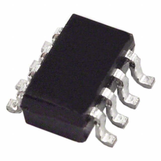
- Part No.:
- AD5273BRJZ1-R2
- Manufacturer:
- Analog Devices Inc.
- Category:
- Digital Potentiometers
- Package:
- SOT-23-8
- Datasheet:
-
 AD5273BRJZ1-R2.pdf
- Description:
- IC DGTL POT 1KOHM 64TAP SOT23-8
- Quantity:
- Payment:

- Shipping:

Inventory:4,455
Please send an inquiry. Send us your inquiry, and we will respond immediately.
Product details
Overview
AD5273BRJZ1-R2 from Analog Devices is a 64-position, one-time programmable (OTP) digital potentiometer in an 8-lead SOT-23 package, featuring 10 kΩ end-to-end resistance, I²C-compatible interface, 5 µA max supply current, and −40°C to +105°C operation. It replaces mechanical trimmers in factory-set calibration circuits where permanent resistance values are required after unlimited pre-programming adjustments.
For engineers reviewing the AD5273BRJZ1-R2 datasheet, AD5273BRJZ1-R2 pinout, AD5273BRJZ1-R2 application, or AD5273BRJZ1-R2 equivalent, key selection criteria include OTP validation status (E1/E0 bits), VDD_OTP programming voltage window (5.0–5.5 V), rheostat/potentiometer mode linearity (±0.5 LSB INL), fuse blow timing (400 ms), and terminal voltage range (GND to VDD).
Technical Context
The AD5273BRJZ1-R2 implements fuse-link-based OTP memory with six data fuses, one test fuse, and one programming lock fuse. Its I²C interface supports up to 400 kHz clock frequency and uses AD0 for dual-device addressing on a shared bus.
It operates in two analog configurations: rheostat mode (W–B or W–A only) and potentiometer mode (A–W–B divider), with guaranteed monotonicity and code-dependent temperature coefficients-300 ppm/°C in rheostat mode and as low as 10 ppm/°C in potentiometer mode at midscale.
Key Specifications
| Parameter | Value and Actual Design Meaning |
|---|---|
| Resolution | 6-bit (64 positions), enabling precise 1.56% step resolution across full scale |
| End-to-End Resistance | 10 kΩ ±30%, defining nominal wiper travel range and current-handling capability |
| Supply Voltage Range | 2.7 V to 5.5 V for normal operation; 5.0–5.5 V required for OTP programming |
| Interface | I²C-compatible, 400 kHz max clock, with AD0 address bit supporting two devices per bus |
| Settling Time | 5 µs typical during power-up and after OTP activation, critical for fast system initialization |
| Operating Temperature | −40°C to +105°C, qualifying for industrial and automotive under-hood environments |
| Power Consumption | 5 µA max IDD, enabling battery-powered calibration systems with multi-year standby life |
Pinout & Package
AD5273BRJZ1-R2 is housed in a compact 8-lead SOT-23 package (JEDEC MO-178AA), measuring 2.9 mm × 1.6 mm × 1.1 mm, with gull-wing leads and standard surface-mount footprint.
| Pin/Terminal | Circuit Role | Design Meaning |
|---|---|---|
| W | Wiper output | Analog output node connecting to internal resistor ladder; voltage ranges from GND to VDD |
| VDD | Positive supply | 2.7–5.5 V for operation; must be 5.0–5.5 V with ≥100 mA sourcing capability for OTP programming |
| GND | Ground reference | Common return for analog and digital sections; required for proper fuse-blow validation |
| SCL | I²C clock input | Open-drain input requiring external pull-up; VIH ≥ 0.7×VDD for reliable communication |
| SDA | I²C bidirectional data | Open-drain I/O with acknowledge; carries write commands (T-bit, data bits) and read-back validation bits (E1/E0) |
| AD0 | Device address bit | Selects between two AD5273 units on same I²C bus; logic high sets slave address to 0x2D, low to 0x2C |
| B | Resistor terminal B | Low-side end of resistor string; used with W in rheostat mode or as ground reference in divider mode |
| A | Resistor terminal A | High-side end of resistor string; connects to VDD or signal source in both operating modes |
Key Features
| Feature | Design Value |
|---|---|
| One-time programmable (OTP) memory | Fuse-link technology enables permanent, tamper-resistant resistance setting after factory calibration |
| OTP validation check | E1/E0 status bits readable via I²C confirm successful fuse blow (1,1) or failure (1,0), eliminating post-program verification hardware |
| Ultralow quiescent current | 5 µA max IDD allows integration into always-on sensor front-ends without measurable battery drain |
| Fast power-up settling | 5 µs settling ensures immediate analog readiness after cold start, avoiding system boot delays |
| Wide supply voltage range | 2.7–5.5 V operation supports direct connection to 3.3 V or 5 V microcontroller I/O rails without level shifters |
Applications
| Factory Sensor Calibration | Industrial Transducer Trim |
|---|---|
Use Scenario: Permanent gain/offset correction applied to pressure or temperature sensor outputs during final test. IC Role / Device Role / Timing Role: Acts as a set-and-forget rheostat in feedback path of op-amp amplifier, fixing transfer function post-calibration. Use Value: Eliminates epoxy-sealed mechanical trimmers, reducing manual labor and long-term drift while maintaining 0.5 LSB linearity over temperature. | Use Scenario: Adjusting zero-point and span of 4–20 mA current loop transmitters before shipment. IC Role / Device Role / Timing Role: Functions as a potentiometer-mode voltage divider controlling DAC reference or op-amp bias point. Use Value: Enables automated, software-driven calibration with I²C; OTP lock prevents field tampering or accidental reprogramming. |
| Programmable Filter Tuning | Embedded System Level Settings |
Use Scenario: Setting cutoff frequency of anti-aliasing or reconstruction filters in data acquisition modules. IC Role / Device Role / Timing Role: Configures RC time constant in active filter topology using 1 kΩ variant (6 MHz BW supported). Use Value: Achieves repeatable, production-grade filter response without component tolerance stacking or hand-tuning. | Use Scenario: Storing board-specific configuration (e.g., display brightness, audio volume, power rail thresholds) during manufacturing. IC Role / Device Role / Timing Role: Provides nonvolatile resistance value for analog input scaling or bias generation in MCU-based control systems. Use Value: Replaces EEPROM + external resistor network, reducing BOM count and PCB area while ensuring parameter retention across power cycles. |
Equivalent & Alternatives
The following parts are listed as comparable options for similar digital potentiometer applications.
| Alternative Part | Technical Difference | Application Difference | Selection Advice |
|---|---|---|---|
| AD5231BRUZ10 | Nonvolatile EEMEM (1024 positions), 10 kΩ, SPI interface, 3 V–5.5 V supply | Supports dynamic field updates; lacks OTP security and fuse validation | Choose when recalibration or user-adjustable settings are required post-deployment |
| MCP45HV51-103E/MS | High-voltage (18 V) OTP digital pot, 10 kΩ, I²C, 128 positions, SOT-23-8 | Rated for higher terminal voltages (up to 18 V); no OTP validation bits or dedicated VDD_OTP pin | Choose for applications exceeding 5.5 V across A/B terminals, accepting reduced diagnostic visibility |
Compared with AD5273BRJZ1-R2, AD5231BRUZ10 offers field reprogrammability but requires additional EEPROM management overhead, while MCP45HV51-103E/MS extends voltage range at the cost of OTP status verification-making AD5273BRJZ1-R2 optimal for secure, verified factory-set calibrations within 5.5 V limits.
Availability
AD5273BRJZ1-R2 is available at Aetrix Electronics and suitable for factory calibration systems, industrial transducer trimming, programmable filter tuning, and embedded system level settings requiring stable component supply and guaranteed OTP integrity.
Supply support for AD5273BRJZ1-R2 includes scheduled delivery planning, volume procurement assistance, BOM continuity management, traceable sourcing, and lifecycle availability coordination for OEM customers, industrial embedded developers, connected-device designers, and electronics production programs.
Manufacturer
Analog Devices, Inc. is a global leader in high-performance analog, mixed-signal, and digital signal processing semiconductors, headquartered in Norwood, MA.
The AD5273 belongs to Analog Devices' precision digital potentiometer product line, designed specifically for factory-programmed, set-and-forget calibration tasks where permanent, verified resistance values replace mechanical trimmers in harsh environments.
FAQ
What is the OTP programming voltage requirement for AD5273BRJZ1-R2?
The AD5273BRJZ1-R2 requires a dedicated OTP programming supply (VDD_OTP) of 5.0 V to 5.5 V, capable of delivering ≥100 mA for 400 ms. This differs from its normal operating supply (2.7–5.5 V). Applying OTP voltage outside this window risks incomplete fuse blow or device damage. The AD5273BRJZ1-R2 datasheet specifies that VDD_OTP must be stable and well-decoupled during programming to ensure reliable OTP activation.
How do I verify successful OTP programming of AD5273BRJZ1-R2?
After OTP programming, read back the E1 and E0 validation bits via I²C read mode. AD5273BRJZ1-R2 returns E1=1, E0=1 on successful fuse blow; E1=1, E0=0 indicates fatal error (discard unit); E1=0, E0=1 is reserved for factory test. These bits are latched permanently and persist across power cycles. The AD5273BRJZ1-R2 does not support reprogramming once E1/E0 = 1/1 is confirmed.
Can AD5273BRJZ1-R2 operate in both rheostat and potentiometer modes?
Yes, AD5273BRJZ1-R2 supports both configurations. In rheostat mode, use W and either A or B terminal (leaving the other open or shorted to W); in potentiometer mode, connect A, W, and B to form a three-terminal voltage divider. Linearity specifications differ: rheostat mode has ±0.5 LSB R-INL (10 kΩ), while potentiometer mode achieves ±0.5 LSB INL. The AD5273BRJZ1-R2's internal fuse structure and register mapping remain identical across both modes.
What is the maximum bandwidth achievable with AD5273BRJZ1-R2?
Bandwidth depends on end-to-end resistance: AD5273BRJZ1-R2 achieves 6 MHz (−3 dB) with 1 kΩ configuration, 600 kHz with 10 kΩ, 110 kHz with 50 kΩ, and 60 kHz with 100 kΩ. These values are measured at code 0x20 and assume VDD = 5 V. The AD5273BRJZ1-R2's bandwidth scales inversely with resistance due to parasitic capacitance (CA/CB = 25 pF, CW = 55 pF), making lower RAB values optimal for high-frequency filter or signal-path applications.
Does AD5273BRJZ1-R2 require external pull-up resistors on SDA and SCL lines?
Yes, AD5273BRJZ1-R2 requires external pull-up resistors on both SDA and SCL lines because its I²C interface uses open-drain outputs. Pull-ups must be connected to VDD (not another voltage rail) to meet VIH ≥ 0.7×VDD. Typical values range from 2.2 kΩ to 10 kΩ depending on bus capacitance and speed requirements. Without proper pull-ups, AD5273BRJZ1-R2 will fail I²C communication and cannot execute write or read operations-including OTP validation bit checks.
AD5273BRJZ1-R2 Specifications
- Product attributes
- Attribute value
- Manufacturer:
- Analog Devices Inc.
- Series:
- -
- Package/Case:
- SOT-23-8
- Packaging:
- Tape & Reel (TR)
- Product Status:
- Discontinued at Digi-Key
- Programmable:
- Not Verified
- Taper:
- Linear
- Configuration:
- Potentiometer
- Number of Circuits:
- 1
- Number of Taps:
- 64
- Resistance (Ohms):
- 1k
- Interface:
- I2C
- Memory Type:
- OTP
- Voltage - Supply:
- 2.7V ~ 5.5V
- Features:
- Selectable Address
- Tolerance:
- ±30%
- Temperature Coefficient (Typ):
- 300ppm/°C
- Mounting Type:
- Surface Mount
- Grade:
- -
- Qualification:
- -
- Supplier Device Package:
- SOT-23-8
- Operating Temperature:
- -40°C ~ 105°C
- Resistance - Wiper (Ohms) (Typ):
- 60
AD5273BRJZ1-R2 FAQ
1.How can I place an order for AD5273BRJZ1-R2 through Aetrix?
Please submit a Request for Quotation (RFQ) for AD5273BRJZ1-R2 on Aetrix. Our sales agent will provide a competitive quotation and guide you through the order confirmation once you accept the terms.
2.Are the price and stock information for AD5273BRJZ1-R2 reliable?
The price and inventory of AD5273BRJZ1-R2 are updated periodically and may fluctuate due to market conditions. Stock and pricing data are typically refreshed every 24 hours. Quotation validity for AD5273BRJZ1-R2 is usually 5 days.
3.What payment methods are accepted for AD5273BRJZ1-R2?
We accept Wire Transfer, PayPal, Credit Card, Western Union, MoneyGram, and Escrow for AD5273BRJZ1-R2 transactions.
Note: Certain payment methods may incur a processing fee.
4.How is shipping managed for AD5273BRJZ1-R2?
AD5273BRJZ1-R2 orders can be shipped via leading logistics carriers, including DHL, UPS, FedEx, TNT, or Registered Mail.
Once your AD5273BRJZ1-R2 order is processed, you will receive an email with the shipment details and tracking number.
Note: Tracking information may take up to 24 hours to appear. Express delivery typically takes 3–5 business days.
5.How can I obtain technical support or documentation for AD5273BRJZ1-R2?
For technical support, including AD5273BRJZ1-R2 datasheets, pinout diagrams, or application guidance, please contact our engineering support team. They can provide detailed documentation and assistance for your AD5273BRJZ1-R2 requirements.
6.How does Aetrix verify that AD5273BRJZ1-R2 is sourced from the original manufacturer or authorized distributors?
All AD5273BRJZ1-R2 products on Aetrix are procured from qualified distributors and authorized channels. Our dedicated quality assurance team conducts strict verification, including traceability checks and, if necessary, third-party testing. This ensures that AD5273BRJZ1-R2 meets industry standards.
7.What is the process for return or replacement of AD5273BRJZ1-R2?
All AD5273BRJZ1-R2 units undergo pre-shipment inspection (PSI). If there is an issue with AD5273BRJZ1-R2, returns or replacements are accepted under the following conditions:
1.Quantity discrepancies, incorrect items, or visible external defects (such as breakage or corrosion), acknowledged by Aetrix.
2.The issue is reported within 90 days of delivery.
3.The AD5273BRJZ1-R2 part is unused and in its original packaging.
Return procedure for AD5273BRJZ1-R2:
1.Submit a request within 90 days.
2.Obtain a Return Material Authorization (RMA) from Aetrix.
AD5273BRJZ1-R2 Tags
-
MCP4018T-103E/LT
Microchip Technology
-
MCP4018T-503E/LT
Microchip Technology

-
MCP4011T-103E/SN
Microchip Technology
-
MCP4018T-104E/LT
Microchip Technology
-
MCP4017T-503E/LT
Microchip Technology
-
MCP4018T-502E/LT
Microchip Technology
-
MCP4017T-103E/LT
Microchip Technology

-
MCP4531T-103E/MF
Microchip Technology
-
MCP4021T-202E/SN
Microchip Technology

-
MCP4023T-103E/CH
Microchip Technology
-
MCP4022T-503E/CH
Microchip Technology

-
MCP4551T-502E/MS
Microchip Technology
Tech Hub

A practical engineering guide to 3.3V and 5V logic compatibility, input thresholds, resistor dividers, translator ICs, MOSFET level shifting, I2C pull-ups, timing limits and power-sequencing risks.

The 74HC595 uses push-pull logic outputs, while the TPIC6B595 uses 50 V open-drain DMOS sinks for higher-power loads. This guide compares timing, current limits, 3.3 V interfacing, load wiring, thermal…

The 74HC595 converts serial data into eight stable parallel outputs. This guide covers pin functions, shift and storage timing, OE and MR behavior, drive-current limits, cascading, voltage compatibilit…

A technical comparison of level-sensitive latches and edge-triggered flip-flops, covering timing windows, setup and hold limits, master–slave operation, time borrowing, race-through, HDL inference and…

A D latch stores one bit while Enable controls when data can pass. This reference covers gate-level operation, truth tables, transparency, setup and hold timing, LE versus OE, common ICs and practical …

An SR latch stores one bit through cross-coupled feedback. This engineering reference covers NOR and NAND implementations, truth tables, forbidden-state recovery, gated operation, switch debouncing, fa…

Latch circuits retain one bit through feedback. This technical reference covers SR and D latches, truth tables, transparency, timing limits, latch-versus-flip-flop behavior, applications and common log…

An engineering guide to LED driver operation, constant-current and constant-voltage outputs, linear and switching topologies, dimming, IC selection, calculations, replacement compatibility, and fault c…

Operational amplifier guide covering op amp basics, feedback, ideal vs real op amps, common configurations, buffer circuits, offset, bias current, gain-bandwidth, slew rate, rail-to-rail limits and sel…

Jumper cables guide covering safe connection order, red and black clamp placement, final ground connection, cable gauge, length, clamp quality, copper vs CCA cables, jump starter comparison and battery…


