
 My Inquiry
 My Account


Analog Devices Inc. AD5750-1BCPZ
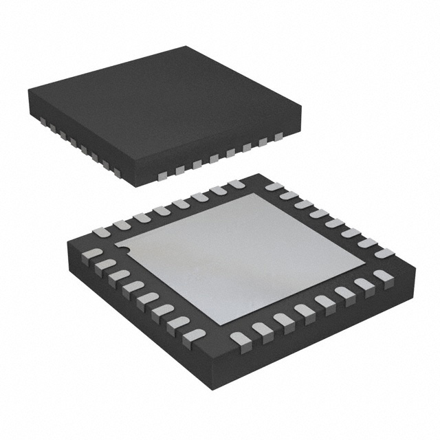
- Part No.:
- AD5750-1BCPZ
- Manufacturer:
- Analog Devices Inc.
- Category:
- Instrumentation, Op Amps, Buffer Amps
- Package:
- 32-WFQFN Exposed Pad, CSP
- Datasheet:
-
 AD5750-1BCPZ.pdf
- Description:
- IC INST AMP 1 CIRCUIT 32LFCSP
- Quantity:
- Payment:

- Shipping:

Inventory:837
Please send an inquiry. Send us your inquiry, and we will respond immediately.
Product details
Overview
AD5750-1BCPZ from Analog Devices is a single-channel, precision industrial current/voltage output driver with software-programmable ranges. It supports five current ranges (including 4 mA to 20 mA and ±24 mA) and four voltage ranges (0 V to 10 V, ±10 V, etc.) with 20% overrange, ±0.03% FSR TUE for current, ±0.02% FSR TUE for voltage, and operates from −40°C to +105°C in a 32-lead 5 mm × 5 mm LFCSP package - deployed in PLC analog output modules.
For engineers reviewing the AD5750-1BCPZ datasheet, AD5750-1BCPZ pinout, AD5750-1BCPZ application, or AD5750-1BCPZ equivalent, key selection criteria include programmable unipolar/bipolar I/V ranges, on-chip fault detection (open/short-circuit), SPI/MICROWIRE interface with CRC-8 PEC, ±12 V to ±24 V dual supply operation, and compliance to AVDD − 2.75 V loop headroom.
Technical Context
The AD5750-1BCPZ implements a dual-path analog output architecture: one path conditions buffered VIN (0 V to 2.5 V) for precision current output via internal or external RSET, while the other routes scaled voltage to VOUT with independent short-circuit protection. Its hardware/software mode selection (via HW SELECT pin) determines whether range configuration is set by digital registers or discrete logic levels on R0–R3.
It integrates real-time fault monitoring - including open-circuit (IFAULT), short-circuit (VFAULT), and overtemperature (TEMP) alerts - with asynchronous CLEAR for zero/midscale reset and power-on-reset ensuring known startup state (0 V or tristate). The device uses a dedicated VSENSE+ and VSENSE− pair for Kelvin sensing of voltage load connections, enabling accurate regulation under varying cable drop.
Key Specifications
| Parameter | Value and Actual Design Meaning |
|---|---|
| Current Output Ranges | 4 mA to 20 mA, 0 mA to 20 mA, 0 mA to 24 mA, ±20 mA, ±24 mA - enables compatibility with 4–20 mA field instruments and bipolar actuator control |
| Voltage Output Ranges | 0 V to 5 V, 0 V to 10 V, ±5 V, ±10 V with 20% overrange - supports legacy sensor calibration offsets and extended DAC headroom |
| Total Unadjusted Error (TUE) | ±0.03% FSR (current), ±0.02% FSR (voltage) - ensures high-fidelity signal reproduction without trimming in factory calibration |
| Output Drift | ±5 ppm/°C (current), ±3 ppm/°C (voltage) - maintains accuracy across industrial temperature extremes (−40°C to +105°C) |
| Power Supply Range | AVDD: +12 V to +24 V (±10%), AVSS: −12 V to −24 V (±10%) - matches standard industrial dual-rail supplies |
| Loop Compliance Voltage | 0 V to AVDD − 2.75 V - allows driving 300 Ω loads at full 20 mA with ±24 V supply (up to 21.25 V headroom) |
| Digital Interface | SPI/MICROWIRE-compatible, 3-wire mode, CRC-8 PEC - reduces isolation component count and improves data integrity in noisy plants |
Pinout & Package
AD5750-1BCPZ is housed in a 32-lead, 5 mm × 5 mm LFCSP package with exposed paddle tied to AVSS. Pin functions are mode-dependent (software/hardware), with shared pins like SDO/VFAULT and FAULT/TEMP serving dual roles based on HW SELECT state.
| Pin/Terminal | Circuit Role | Design Meaning |
|---|---|---|
| 1 (SDO/VFAULT) | Serial Data Output / Short-Circuit Fault Alert | In software mode: CMOS SDO for register readback; in hardware mode: open-drain VFAULT asserted low on VOUT short |
| 3 (CLEAR) | Asynchronous Reset Input | Active-high signal forcing output to zero-scale (unipolar) or midscale (bipolar); also defines power-up voltage state when HW SELECT = 0 |
| 6 (SYNC/RSET) | Register Latch / RSET Selection | In software mode: rising edge latches 24-bit input shift register; in hardware mode: selects internal/external current sense resistor |
| 7 (SCLK/OUTEN) | Serial Clock Input / Output Enable | In software mode: falling-edge clock up to 50 MHz; in hardware mode: active-high enable for IOUT/VOUT buffers |
| 15 (VIN) | Analog Input | Buffered 0 V to 2.5 V input range - interfaces directly with low-voltage DACs (e.g., AD5662) without level-shifting |
| 18 (IOUT) | Current Output Terminal | High-side current source capable of driving 300 Ω loads with open/short-circuit protection and fault reporting |
| 23 (VOUT) | Voltage Output Terminal | Buffered, rail-to-rail-capable output with Kelvin sense (VSENSE+/VSENSE−) for remote load regulation |
| 29 (HW SELECT) | Mode Configuration Input | Logic low = software mode (SPI control); logic high = hardware mode (R0–R3 pin-strapped ranges) |
Key Features
| Feature | Design Value |
|---|---|
| Programmable I/V Ranges | Five current and four voltage ranges selectable via SPI registers - eliminates hardware redesign when changing field instrument types |
| On-Chip Fault Detection | Detects open-circuit (IOUT), short-circuit (VOUT), and overtemperature faults with dedicated open-drain alert pins - enables predictive maintenance in distributed I/O systems |
| Packet Error Checking (PEC) | CRC-8 checksum on SPI writes - prevents undetected command corruption in electrically noisy industrial environments |
| Flexible Power-Up State | Configurable to start at 0 V or high-impedance tristate - avoids transient surges during system boot in safety-critical loops |
| Kelvin Voltage Sensing | VSENSE+ and VSENSE− inputs compensate for IR drop across long cables - maintains ±0.02% FSR accuracy even with 10 Ω series resistance |
Applications
| PLC Analog Output Module | Process Controller Actuator Drive |
|---|---|
Use Scenario: Modular PLC backplane with isolated analog output slots delivering 4–20 mA signals to valve positioners and transmitters. IC Role / Device Role / Timing Role: Precision current driver converting digital setpoints into field-ready loop current; handles range reconfiguration via firmware update. Use Value: Eliminates manual jumpering or DIP-switch changes during commissioning; supports hot-swappable I/O modules with consistent calibration traceability. |
Use Scenario: Standalone DIN-rail process controller regulating temperature via 0–10 V input to SSRs or 4–20 mA input to pneumatic positioners. IC Role / Device Role / Timing Role: Dual-mode output stage providing either voltage or current per channel, synchronized to controller's scan cycle via SPI write timing. Use Value: Single BOM item covers both voltage- and current-driven final control elements, reducing inventory and qualification effort. |
| Industrial Data Acquisition System | Hazardous Area Signal Conditioner |
Use Scenario: Rack-mounted DAQ unit acquiring sensor data and retransmitting calibrated analog outputs to legacy recorders or chart drives. IC Role / Device Role / Timing Role: High-accuracy voltage/current translator with 20% overrange - accommodates sensor drift and calibration offsets without clipping. Use Value: Maintains ±0.02% FSR TUE across −40°C to +105°C ambient, enabling direct mounting near heat-generating equipment. |
Use Scenario: Intrinsically safe barrier module in Zone 1/2 installations requiring galvanic isolation and fault-safe shutdown. IC Role / Device Role / Timing Role: Current output stage with integrated open/short-circuit detection feeding isolated barrier ICs; CLEAR pin used for fail-safe zeroing. Use Value: Reduces external fault-handling circuitry; PEC-enabled SPI allows diagnostics over isolated UART links without compromising SIL-2 compliance. |
Equivalent & Alternatives
The following parts are listed as comparable options for similar industrial I/V output driver applications.
| Alternative Part | Technical Difference | Application Difference | Selection Advice |
|---|---|---|---|
| AD5751 | Single-supply operation (up to +55 V AVDD), no AVSS rail required; lower TUE (±0.015% FSR) but no voltage output channel | Used where only current output is needed and board space is constrained; lacks dual I/V capability of AD5750-1BCPZ | Select AD5751 when simplifying power design outweighs need for voltage output flexibility |
| AD5422 | Integrated 16-bit DAC + current source/voltage output; higher integration but fixed 4–20 mA range and no software-programmable voltage ranges | Preferred in compact loop-powered transmitters where DAC and driver co-location reduces noise; less flexible for multi-range field devices | Choose AD5422 when end-to-end DAC-to-loop conversion is required and range agility is secondary |
Compared with AD5750-1BCPZ, AD5751 offers simpler power architecture but sacrifices voltage output versatility, while AD5422 embeds the DAC but locks range configuration - making AD5750-1BCPZ optimal for modular, firmware-reconfigurable analog output systems requiring both precision current and voltage modes.
Availability
AD5750-1BCPZ is available at Aetrix Electronics and suitable for PLC analog output modules, process controller actuator drives, and industrial data acquisition systems requiring stable component supply, long-term lifecycle support, and guaranteed traceable sourcing.
Supply support for AD5750-1BCPZ includes scheduled delivery planning, volume procurement assistance, BOM continuity management, traceable sourcing, and lifecycle availability coordination for OEM customers, industrial embedded developers, connected-device designers, and electronics production programs.
Manufacturer
Analog Devices is a global leader in high-performance analog, mixed-signal, and digital signal processing semiconductors, serving industrial, automotive, communications, and healthcare markets since 1965.
The AD5750 family was designed specifically for industrial process control and programmable logic controller analog output stages, emphasizing configurability, fault resilience, and wide-temperature accuracy without external trimming.
FAQ
What is the input voltage range for AD5750-1BCPZ?
The AD5750-1BCPZ accepts a buffered analog input (VIN) of 0 V to 2.5 V - optimized for interfacing with low-voltage, single-supply DACs such as the AD5662. This range differs from the AD5750 (0 V to 4.096 V) and AD5750-2 (0 V to 2.5 V), confirming AD5750-1BCPZ's specific role in cost-sensitive, 2.5 V reference-based systems. The input leakage current is tightly controlled at ±1 µA.
Does AD5750-1BCPZ support both current and voltage outputs simultaneously?
No - the AD5750-1BCPZ provides either current output (IOUT pin) or voltage output (VOUT pin) at any given time, not concurrently. Its architecture separates the two paths: current output uses internal/external RSET and IOUT, while voltage output uses the dedicated VOUT buffer with Kelvin sensing (VSENSE+/VSENSE−). Both cannot be active simultaneously due to shared bias structures and fault-monitoring logic.
How does the HW SELECT pin affect AD5750-1BCPZ operation?
The HW SELECT pin configures AD5750-1BCPZ into hardware mode (logic high) or software mode (logic low). In software mode, all functions - including output range, fault behavior, and overrange - are controlled via SPI registers. In hardware mode, range selection is determined by R0–R3 pin states, and features like PEC and register readback are disabled. This dual-mode capability supports both firmware-flexible and pin-strapped deployments.
What fault conditions does AD5750-1BCPZ detect and report?
The AD5750-1BCPZ detects and reports three primary fault conditions: open-circuit on IOUT (via IFAULT in hardware mode or FAULT/TEMP in software mode), short-circuit on VOUT (via VFAULT), and overtemperature (via FAULT/TEMP or NC/IFAULT depending on mode). All fault alerts are open-drain outputs requiring external pull-up resistors and assert low upon detection - enabling immediate system-level response without polling.
Can AD5750-1BCPZ drive inductive loads like solenoid valves?
Yes - the AD5750-1BCPZ is rated to drive inductive loads up to 0.1 H, with built-in protection against flyback voltage transients. When driving such loads, proper external compensation (e.g., snubber networks or clamping diodes) is required, and the COMP1/COMP2 pins may be used to stabilize the VOUT buffer if capacitive loading exceeds 1 nF. The current output stage includes slew-rate limiting to suppress ringing during step transitions.
AD5750-1BCPZ Specifications
- Product attributes
- Attribute value
- Manufacturer:
- Analog Devices Inc.
- Series:
- -
- Package/Case:
- 32-WFQFN Exposed Pad, CSP
- Packaging:
- Tray
- Product Status:
- Active
- Amplifier Type:
- Instrumentation
- Number of Circuits:
- 1
- Output Type:
- -
- Slew Rate:
- 2V/µs
- Gain Bandwidth Product:
- -
- -3db Bandwidth:
- -
- Current - Input Bias:
- -
- Voltage - Input Offset:
- -
- Current - Supply:
- 5.2mA
- Current - Output / Channel:
- 24 mA
- Voltage - Supply Span (Min):
- 24 V
- Voltage - Supply Span (Max):
- 48 V
- Operating Temperature:
- -40°C ~ 105°C
- Grade:
- -
- Qualification:
- -
- Mounting Type:
- Surface Mount
- Supplier Device Package:
- 32-LFCSP-WQ (5x5)
AD5750-1BCPZ FAQ
1.How can I place an order for AD5750-1BCPZ through Aetrix?
Please submit a Request for Quotation (RFQ) for AD5750-1BCPZ on Aetrix. Our sales agent will provide a competitive quotation and guide you through the order confirmation once you accept the terms.
2.Are the price and stock information for AD5750-1BCPZ reliable?
The price and inventory of AD5750-1BCPZ are updated periodically and may fluctuate due to market conditions. Stock and pricing data are typically refreshed every 24 hours. Quotation validity for AD5750-1BCPZ is usually 5 days.
3.What payment methods are accepted for AD5750-1BCPZ?
We accept Wire Transfer, PayPal, Credit Card, Western Union, MoneyGram, and Escrow for AD5750-1BCPZ transactions.
Note: Certain payment methods may incur a processing fee.
4.How is shipping managed for AD5750-1BCPZ?
AD5750-1BCPZ orders can be shipped via leading logistics carriers, including DHL, UPS, FedEx, TNT, or Registered Mail.
Once your AD5750-1BCPZ order is processed, you will receive an email with the shipment details and tracking number.
Note: Tracking information may take up to 24 hours to appear. Express delivery typically takes 3–5 business days.
5.How can I obtain technical support or documentation for AD5750-1BCPZ?
For technical support, including AD5750-1BCPZ datasheets, pinout diagrams, or application guidance, please contact our engineering support team. They can provide detailed documentation and assistance for your AD5750-1BCPZ requirements.
6.How does Aetrix verify that AD5750-1BCPZ is sourced from the original manufacturer or authorized distributors?
All AD5750-1BCPZ products on Aetrix are procured from qualified distributors and authorized channels. Our dedicated quality assurance team conducts strict verification, including traceability checks and, if necessary, third-party testing. This ensures that AD5750-1BCPZ meets industry standards.
7.What is the process for return or replacement of AD5750-1BCPZ?
All AD5750-1BCPZ units undergo pre-shipment inspection (PSI). If there is an issue with AD5750-1BCPZ, returns or replacements are accepted under the following conditions:
1.Quantity discrepancies, incorrect items, or visible external defects (such as breakage or corrosion), acknowledged by Aetrix.
2.The issue is reported within 90 days of delivery.
3.The AD5750-1BCPZ part is unused and in its original packaging.
Return procedure for AD5750-1BCPZ:
1.Submit a request within 90 days.
2.Obtain a Return Material Authorization (RMA) from Aetrix.
AD5750-1BCPZ Tags

-
LM358DT
STMicroelectronics

-
LM358DR
Texas Instruments
-
LM2904DR
Texas Instruments
-
LM358ADR
Texas Instruments

-
LM2904DGKR
Texas Instruments

-
LM324DR
Texas Instruments

-
MCP6006T-E/OT
Microchip Technology
-
MCP6006UT-E/OT
Microchip Technology

-
LM324PWR
Texas Instruments
-
LM2902PWR
Texas Instruments
-
LM2902DR
Texas Instruments

-
LM358P
Texas Instruments
Tech Hub

A practical engineering guide to 3.3V and 5V logic compatibility, input thresholds, resistor dividers, translator ICs, MOSFET level shifting, I2C pull-ups, timing limits and power-sequencing risks.

The 74HC595 uses push-pull logic outputs, while the TPIC6B595 uses 50 V open-drain DMOS sinks for higher-power loads. This guide compares timing, current limits, 3.3 V interfacing, load wiring, thermal…

The 74HC595 converts serial data into eight stable parallel outputs. This guide covers pin functions, shift and storage timing, OE and MR behavior, drive-current limits, cascading, voltage compatibilit…

A technical comparison of level-sensitive latches and edge-triggered flip-flops, covering timing windows, setup and hold limits, master–slave operation, time borrowing, race-through, HDL inference and…

A D latch stores one bit while Enable controls when data can pass. This reference covers gate-level operation, truth tables, transparency, setup and hold timing, LE versus OE, common ICs and practical …

An SR latch stores one bit through cross-coupled feedback. This engineering reference covers NOR and NAND implementations, truth tables, forbidden-state recovery, gated operation, switch debouncing, fa…

Latch circuits retain one bit through feedback. This technical reference covers SR and D latches, truth tables, transparency, timing limits, latch-versus-flip-flop behavior, applications and common log…

An engineering guide to LED driver operation, constant-current and constant-voltage outputs, linear and switching topologies, dimming, IC selection, calculations, replacement compatibility, and fault c…

Operational amplifier guide covering op amp basics, feedback, ideal vs real op amps, common configurations, buffer circuits, offset, bias current, gain-bandwidth, slew rate, rail-to-rail limits and sel…

Jumper cables guide covering safe connection order, red and black clamp placement, final ground connection, cable gauge, length, clamp quality, copper vs CCA cables, jump starter comparison and battery…


