
 My Inquiry
 My Account


Analog Devices Inc. AD6140ARSRL
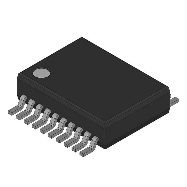
- Part No.:
- AD6140ARSRL
- Manufacturer:
- Analog Devices Inc.
- Category:
- Analog to Digital Converters (ADC)
- Package:
- 20-SSOP (0.209", 5.30mm Width)
- Datasheet:
-
 AD6140ARSRL.pdf
- Description:
- BANDPASS IF SUBSYSTEM
- Quantity:
- Payment:

- Shipping:

Inventory:3,000
Please send an inquiry. Send us your inquiry, and we will respond immediately.
Product details
Overview
AD6140ARSRL from Analog Devices is a bandpass sigma-delta (Σ∆) IF subsystem IC designed for high-dynamic-range digital radio receivers. It integrates a variable-gain preamplifier (16–29.5 dB), mixer, AGC detector, 6.144 MHz ECL-input Σ∆ modulator, ECL-to-CMOS clock translator, and LNA bias amplifier - all in a single 20-lead SSOP package operating at 2.7 V with 4.8 mA supply current. It targets FLEX™/ReFLEX™ multimode receiver front-ends.
For engineers reviewing the AD6140ARSRL datasheet, AD6140ARSRL pinout, AD6140ARSRL application, or AD6140ARSRL equivalent, key selection considerations include its 192 kHz center-frequency bandpass modulation, 83 dB dynamic range (6.25 kHz BW), –27 dBm input IP3, 10.5 dB noise figure, and AGC time-constant selectability via logic-controlled charging current (2.8 µA / 50 nA).
Technical Context
The AD6140ARSRL implements a fixed-frequency IF signal chain: it accepts a 49.6 MHz IF input and 49.792/49.408 MHz LO to produce a 192 kHz bandpass Σ∆ bitstream output. Its internal AGC loop adjusts preamplifier gain over 13 dB using a voltage-controlled integrator with externally selectable time constant (fast/slow modes).
It features dual-domain power supplies (AVDD/DVDD), separate analog/digital/translator grounds (AGND/DGND/BUFFER_GND), and a dedicated 1 V reference input for ADC accuracy. The ECL-to-CMOS level shifter converts 6.144 MHz differential ECL clock inputs to single-ended CMOS outputs (D_CLOCK_OUT) while driving 5 pF loads with ±2.5% asymmetry.
Key Specifications
| Parameter | Value and Actual Design Meaning |
|---|---|
| Supply Voltage | 2.7 V nominal; operates across 2.5–2.9 V - ensures compatibility with low-voltage industrial power rails. |
| Supply Current | 4.8 mA typical at 2.7 V - enables ultralow-power operation in battery-sensitive multimode receivers. |
| Dynamic Range | 83 dB typical in 6.25 kHz bandwidth centered at 192 kHz - supports high-fidelity digitization of narrowband IF signals. |
| Noise Figure | 10.5 dB at max gain with external termination - defines minimum detectable signal level in receiver front-end design. |
| Input IP3 | –19 dBm typical - quantifies linearity under two-tone conditions; critical for adjacent-channel interference rejection. |
| AGC Range | 13 dB - enables automatic adaptation to varying RF signal strength without manual gain staging. |
| Output Data Format | Single-bit 6.144 MHz Σ∆ bitstream (CMOS) - requires external decimation filter for multibit conversion. |
Pinout & Package
AD6140ARSRL is housed in a 20-lead plastic Shrink Small Outline Package (SSOP), RoHS-compliant, with 0.65 mm lead pitch and dimensions 7.50 mm × 5.38 mm × 1.78 mm (max height). Pin 1 identifier located at top-left corner per JEDEC MO-153 standard.
| Pin/Terminal | Circuit Role | Design Meaning |
|---|---|---|
| 1 (LNA_FORCE) | LNA bias output | Drives discrete LNA gate; 0–2.7 V range enables ON/OFF and gain control of external amplifier. |
| 2 (LNA_SENSE) | LNA bias feedback input | Monitors LNA drain/source node; sets closed-loop bias point within VDD to VDD–0.3 V range. |
| 3,4 (CLK_IN+, CLK_IN–) | Differential ECL clock input | Accepts 6.144 MHz, 800 mV p-p ECL signal; direct-coupled into 1500 Ω impedance for precise timing alignment. |
| 5 (BUFFER_GND) | ECL-to-CMOS translator ground | Dedicated ground return for level-shifter circuitry - isolates digital switching noise from analog sections. |
| 6 (Σ∆_DATA_OUT) | Σ∆ modulator serial data output | CMOS-level 6.144 MHz single-bit stream - interfaces directly to FPGA or ASIC decimation logic. |
| 7 (Σ∆_CLOCK_OUT) | Translated system clock output | CMOS 6.144 MHz clock synchronized to data; drives 5 pF load with ±2.5% duty-cycle asymmetry. |
| 9 (POWER_DOWN) | Power enable control | Active-low logic input; transitions to 3 µA standby in <100 µs - enables rapid sleep/wake cycling. |
| 10 (AGC_TC_SELECT) | AGC time constant mode select | Logic-controlled switch between fast (2.8 µA) and slow (50 nA) AGC capacitor charging currents - ratio 56:1. |
| 13 (AGC_CAPACITOR) | AGC integrator node | External capacitor connection point (e.g., 0.1 µF); sets AGC loop response time per T = CV/I equation. |
| 19 (IF_INPUT) | IF signal input | 2.5 kΩ || 12 pF input impedance at 49.6 MHz - requires matching network for 50 Ω source termination. |
Key Features
| Feature | Design Value |
|---|---|
| Integrated bandpass Σ∆ modulator | Fixed 192 kHz center frequency with shaped quantization noise - eliminates need for external IF filters before digitization. |
| Variable-gain preamplifier + AGC detector | 13 dB automatic gain control range with selectable time constant - maintains consistent ADC input level across wide RF signal dynamics. |
| ECL-to-CMOS clock translation | On-chip level shifter converts 6.144 MHz differential ECL to single-ended CMOS - removes need for external translator IC and reduces board space. |
| Dual-domain power architecture | Separate AVDD, DVDD, BUFFER_VDD and AGND/DGND/BUFFER_GND - minimizes supply coupling between analog, digital, and clock domains. |
| LNA bias amplifier | Configurable force/sense pair (Pins 1 & 2) - enables stable biasing of discrete GaAs or SiGe LNAs without external op amp. |
Applications
| FLEX™/ReFLEX™ Base Station Receiver | Multimode Paging Receiver Front-End |
|---|---|
Use Scenario: Digitizing 49.6 MHz IF output from crystal filter in Motorola ReFLEX transceiver systems. IC Role / Device Role / Timing Role: Bandpass Σ∆ IF subsystem providing 192 kHz-centered digitization, AGC stabilization, and LNA bias control. Use Value: Enables high-dynamic-range (83 dB) reception with minimal external components - reducing BOM count and layout complexity in licensed-band paging infrastructure. |
Use Scenario: Converting first IF in dual-conversion receivers supporting multiple legacy paging protocols (e.g., POCSAG, FLEX). IC Role / Device Role / Timing Role: Fixed-frequency IF ADC subsystem with integrated mixer, preamp, and AGC - replaces discrete signal chain stages. Use Value: Delivers consistent 10.5 dB noise figure and –19 dBm IP3 across temperature (–40°C to +85°C), ensuring reliable decoding under weak-signal conditions. |
| Low-Power Wide-Area Paging Terminal | Industrial Telemetry IF Interface |
Use Scenario: Battery-powered portable receiver requiring extended operational life and rapid wake-from-sleep capability. IC Role / Device Role / Timing Role: Ultralow-power (4.8 mA active, 3 µA standby) IF digitizer with sub-100 µs power-down response. Use Value: Reduces average current draw during idle periods while maintaining full performance on demand - extends battery life in field-deployed units. |
Use Scenario: Digitizing filtered IF signals in fixed-location telemetry gateways operating in harsh electromagnetic environments. IC Role / Device Role / Timing Role: ESD-hardened (4 kV HBM) IF subsystem with dedicated ground planes and supply isolation. Use Value: Maintains signal integrity in electrically noisy settings via separated AGND/DGND/BUFFER_GND and clean BUFFER_VDD decoupling requirements. |
Equivalent & Alternatives
The following parts are listed as comparable options for similar bandpass IF subsystem applications.
| Alternative Part | Technical Difference | Application Difference | Selection Advice |
|---|---|---|---|
| AD6141ARSRL | Same architecture but optimized for 12.288 MHz clock and 384 kHz center frequency; higher power (6.2 mA). | Targets wider IF bandwidths (e.g., 12.5 kHz) in newer ReFLEX variants - not drop-in compatible due to clock/LO frequency shift. | Select AD6141ARSRL only when redesigning for higher IF sampling rates and broader channel spacing. |
| MAX2102ETM+ | Direct-conversion quadrature demodulator with integrated 10-bit ADC; no Σ∆ modulator or AGC - requires external digital AGC. | Designed for zero-IF architectures; lacks bandpass Σ∆ noise shaping - unsuitable for crystal-filter-based IF sampling. | Choose MAX2102ETM+ only for new zero-IF receiver designs where baseband I/Q digitization is preferred over bandpass IF sampling. |
Compared with AD6140ARSRL, AD6141ARSRL shifts center frequency and clock rate - requiring LO and decimation filter redesign; MAX2102ETM+ abandons bandpass Σ∆ entirely, trading noise-shaping advantage for baseband flexibility and higher ADC resolution.
Availability
AD6140ARSRL is available at Aetrix Electronics and suitable for FLEX™/ReFLEX™ receiver modules, multimode paging terminals, and industrial telemetry IF interfaces requiring stable component supply across extended temperature ranges and long production lifecycles.
Supply support for AD6140ARSRL includes scheduled delivery planning, volume procurement assistance, BOM continuity management, traceable sourcing, and lifecycle availability coordination for OEM customers, industrial embedded developers, connected-device designers, and electronics production programs.
Manufacturer
Analog Devices, Inc. is a global semiconductor company specializing in high-performance analog, mixed-signal, and digital signal processing technologies for precision instrumentation, communications, and industrial applications.
The AD6140ARSRL belongs to Analog Devices' legacy IF subsystem product line, engineered specifically for licensed-band paging receivers requiring bandpass Σ∆ digitization at 192 kHz with integrated AGC and LNA bias control.
FAQ
What is the primary function of the AD6140ARSRL in a receiver signal chain?
The AD6140ARSRL serves as a complete bandpass sigma-delta IF subsystem, converting a 49.6 MHz IF input into a 6.144 MHz single-bit Σ∆ bitstream centered at 192 kHz. It integrates preamplification, mixing, AGC detection, clock translation, and LNA biasing - enabling high-dynamic-range digitization without external modulator or AGC circuitry. Its fixed-frequency architecture makes AD6140ARSRL ideal for standardized paging receiver platforms like Motorola ReFLEX.
Does the AD6140ARSRL support adjustable center frequency or bandwidth?
No - the AD6140ARSRL is a fixed-frequency device optimized exclusively for a 192 kHz center frequency with 6.25 kHz bandwidth (typical dynamic range measurement). Its Σ∆ modulator, mixer LO injection points (49.792/49.408 MHz), and clock input (6.144 MHz) are co-designed for this specific frequency plan. Deviating from these values degrades noise shaping, dynamic range, and linearity - so AD6140ARSRL does not support user-adjustable center frequency or programmable bandwidth.
How does the AGC circuit in the AD6140ARSRL operate, and what external components does it require?
The AD6140ARSRL AGC uses an internal detector that monitors the Σ∆ modulator input level and controls preamplifier gain over 13 dB. It requires an external capacitor on Pin 13 (AGC_CAPACITOR) - typically 0.1 µF per Motorola ReFLEX implementation - and selects fast (2.8 µA) or slow (50 nA) charging current via Pin 10 (AGC_TC_SELECT). No external op amp or resistive divider is needed; the AD6140ARSRL provides full closed-loop AGC with only one capacitor and logic control.
Can the AD6140ARSRL interface directly with an FPGA for decimation filtering?
Yes - the AD6140ARSRL outputs a CMOS-level 6.144 MHz single-bit Σ∆ bitstream on Pin 6 (Σ∆_DATA_OUT) and a synchronized CMOS clock on Pin 7 (Σ∆_CLOCK_OUT), both compatible with standard FPGA I/O banks. Its deterministic timing, ±2.5% clock asymmetry, and 5 pF load drive capability allow direct connection to Xilinx or Intel FPGA fabric for real-time decimation - eliminating level-shifting or buffering for AD6140ARSRL's digital interface.
Is the AD6140ARSRL still in active production, and what is its temperature rating?
The AD6140ARSRL is marked "OBSOLETE" in its official documentation, but remains available through authorized distributors and Aetrix Electronics for legacy support and long-lifecycle industrial programs. It is rated for the industrial temperature range of –40°C to +85°C and specified at 2.7 V supply, making AD6140ARSRL suitable for deployment in uncontrolled outdoor or factory-floor environments where thermal stability is critical.
AD6140ARSRL Specifications
- Product attributes
- Attribute value
- Manufacturer:
- Analog Devices Inc.
- Series:
- AD6140
- Package/Case:
- 20-SSOP (0.209", 5.30mm Width)
- Packaging:
- Bulk
- Product Status:
- Active
- Number of Bits:
- -
- Sampling Rate (Per Second):
- -
- Number of Inputs:
- 1
- Input Type:
- Single Ended
- Data Interface:
- -
- Configuration:
- ADC
- Ratio - S/H:ADC:
- 0:1
- Number of A/D Converters:
- 1
- Architecture:
- Sigma-Delta
- Reference Type:
- External
- Voltage - Supply, Analog:
- 2.5V ~ 2.9V
- Voltage - Supply, Digital:
- 2.5V ~ 2.9V
- Features:
- -
- Operating Temperature:
- -40°C ~ 85°C
- Supplier Device Package:
- 20-SSOP
- Mounting Type:
- Surface Mount
- Grade:
- -
- Qualification:
- -
AD6140ARSRL FAQ
1.How can I place an order for AD6140ARSRL through Aetrix?
Please submit a Request for Quotation (RFQ) for AD6140ARSRL on Aetrix. Our sales agent will provide a competitive quotation and guide you through the order confirmation once you accept the terms.
2.Are the price and stock information for AD6140ARSRL reliable?
The price and inventory of AD6140ARSRL are updated periodically and may fluctuate due to market conditions. Stock and pricing data are typically refreshed every 24 hours. Quotation validity for AD6140ARSRL is usually 5 days.
3.What payment methods are accepted for AD6140ARSRL?
We accept Wire Transfer, PayPal, Credit Card, Western Union, MoneyGram, and Escrow for AD6140ARSRL transactions.
Note: Certain payment methods may incur a processing fee.
4.How is shipping managed for AD6140ARSRL?
AD6140ARSRL orders can be shipped via leading logistics carriers, including DHL, UPS, FedEx, TNT, or Registered Mail.
Once your AD6140ARSRL order is processed, you will receive an email with the shipment details and tracking number.
Note: Tracking information may take up to 24 hours to appear. Express delivery typically takes 3–5 business days.
5.How can I obtain technical support or documentation for AD6140ARSRL?
For technical support, including AD6140ARSRL datasheets, pinout diagrams, or application guidance, please contact our engineering support team. They can provide detailed documentation and assistance for your AD6140ARSRL requirements.
6.How does Aetrix verify that AD6140ARSRL is sourced from the original manufacturer or authorized distributors?
All AD6140ARSRL products on Aetrix are procured from qualified distributors and authorized channels. Our dedicated quality assurance team conducts strict verification, including traceability checks and, if necessary, third-party testing. This ensures that AD6140ARSRL meets industry standards.
7.What is the process for return or replacement of AD6140ARSRL?
All AD6140ARSRL units undergo pre-shipment inspection (PSI). If there is an issue with AD6140ARSRL, returns or replacements are accepted under the following conditions:
1.Quantity discrepancies, incorrect items, or visible external defects (such as breakage or corrosion), acknowledged by Aetrix.
2.The issue is reported within 90 days of delivery.
3.The AD6140ARSRL part is unused and in its original packaging.
Return procedure for AD6140ARSRL:
1.Submit a request within 90 days.
2.Obtain a Return Material Authorization (RMA) from Aetrix.
AD6140ARSRL Tags
-
ADC081C021CIMKX/NOPB
Texas Instruments

-
MCP3021A5T-E/OT
Microchip Technology
-
TLA2024IRUGR
Texas Instruments
-
MCP3221A5T-E/OT
Microchip Technology
-
MCP3221A5T-I/OT
Microchip Technology
-
MCP3221A4T-E/OT
Microchip Technology
-
MCP3221A6T-E/OT
Microchip Technology
-
MCP3221A0T-E/OT
Microchip Technology
-
MCP3221A1T-E/OT
Microchip Technology

-
ADC121S021CIMFX/NOPB
Texas Instruments

-
MCP3001-I/MS
Microchip Technology

-
MCP3001-I/SN
Microchip Technology
Tech Hub

A practical engineering guide to 3.3V and 5V logic compatibility, input thresholds, resistor dividers, translator ICs, MOSFET level shifting, I2C pull-ups, timing limits and power-sequencing risks.

The 74HC595 uses push-pull logic outputs, while the TPIC6B595 uses 50 V open-drain DMOS sinks for higher-power loads. This guide compares timing, current limits, 3.3 V interfacing, load wiring, thermal…

The 74HC595 converts serial data into eight stable parallel outputs. This guide covers pin functions, shift and storage timing, OE and MR behavior, drive-current limits, cascading, voltage compatibilit…

A technical comparison of level-sensitive latches and edge-triggered flip-flops, covering timing windows, setup and hold limits, master–slave operation, time borrowing, race-through, HDL inference and…

A D latch stores one bit while Enable controls when data can pass. This reference covers gate-level operation, truth tables, transparency, setup and hold timing, LE versus OE, common ICs and practical …

An SR latch stores one bit through cross-coupled feedback. This engineering reference covers NOR and NAND implementations, truth tables, forbidden-state recovery, gated operation, switch debouncing, fa…

Latch circuits retain one bit through feedback. This technical reference covers SR and D latches, truth tables, transparency, timing limits, latch-versus-flip-flop behavior, applications and common log…

An engineering guide to LED driver operation, constant-current and constant-voltage outputs, linear and switching topologies, dimming, IC selection, calculations, replacement compatibility, and fault c…

Operational amplifier guide covering op amp basics, feedback, ideal vs real op amps, common configurations, buffer circuits, offset, bias current, gain-bandwidth, slew rate, rail-to-rail limits and sel…

Jumper cables guide covering safe connection order, red and black clamp placement, final ground connection, cable gauge, length, clamp quality, copper vs CCA cables, jump starter comparison and battery…


