
 My Inquiry
 My Account


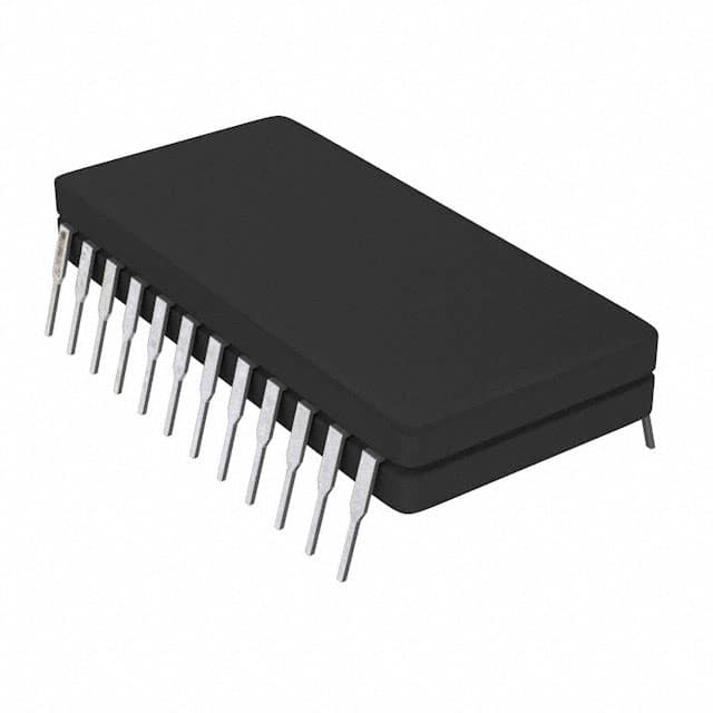
Analog Devices Inc. AD698SQ
- Part No.:
- AD698SQ
- Manufacturer:
- Analog Devices Inc.
- Category:
- Sensor and Detector Interfaces
- Package:
- 24-CDIP (0.600", 15.24mm)
- Datasheet:
-
 AD698SQ.pdf
- Description:
- IC LVDT SGNL COND UNVRSL 24CDIP
- Quantity:
- Payment:

- Shipping:

Inventory:4,223
Please send an inquiry. Send us your inquiry, and we will respond immediately.
Product details
Overview
AD698SQ from Analog Devices is a monolithic LVDT signal conditioner IC that converts mechanical core position into a precise DC output voltage via ratiometric synchronous demodulation. It integrates an oscillator, voltage reference, dual demodulator channels, and computational circuitry - delivering ±11 V output, 0.05% linearity, and operation across –55°C to +125°C in a 24-lead CERDIP package for aerospace and high-reliability industrial position sensing.
For engineers reviewing the AD698SQ datasheet, AD698SQ pinout, AD698SQ application, or AD698SQ equivalent, key selection criteria include its ratiometric A/B transfer function, excitation frequency range (20 Hz–20 kHz), unipolar/bipolar output configurability, ±15 V dual-supply operation, and compatibility with half-bridge and 4-wire series-opposed LVDTs.
Technical Context
The AD698SQ implements a duty-cycle-based divider architecture that computes the ratio of secondary (A) to primary (B) LVDT voltages, eliminating gain errors from oscillator amplitude drift. Its internal multivibrator-driven sine shaper delivers low-distortion excitation (–50 dB THD) with frequency set by a single capacitor and amplitude set by a resistor.
Two independent synchronous demodulation channels process A (LVDT secondary) and B (LVDT primary) inputs; phase compensation pins (+ACOMP/–ACOMP) allow correction of LVDT-induced phase shifts. The output amplifier scales a 500 µA reference current using external R2 to produce a final voltage per VOUT = 500 µA × (A/B) × R2.
Key Specifications
| Parameter | Value and Actual Design Meaning |
|---|---|
| Transfer Function | Ratiometric A/B division - cancels primary drive amplitude drift, enabling stable gain over temperature without calibration. |
| Linearity Error | ±500 ppm of FS (0.05%) - ensures sub-0.1% full-scale deviation across mechanical stroke, critical for precision metrology. |
| Output Voltage Range | ±11 V - supports direct interfacing with industrial PLC analog inputs and data acquisition systems requiring bipolar range. |
| Excitation Frequency | 20 Hz to 20 kHz - configurable via single capacitor (C1), enabling optimization for LVDT zero-phase frequency or mechanical bandwidth. |
| Gain Drift | 20 ppm/°C typ - enables <±0.01% gain shift over –55°C to +125°C, meeting MIL-STD-883 Class B requirements. |
| Operating Temperature | –55°C to +125°C - qualified for extended-range military, downhole, and engine-mounted applications. |
| Supply Voltage | ±13 V to ±18 V dual supply - accommodates standard ±15 V rails with 36 V total supply headroom. |
Pinout & Package
AD698SQ is housed in a hermetically sealed 24-lead CERDIP package (Q-24-2), rated for –55°C to +125°C operation and compatible with high-reliability soldering processes including MIL-STD-202 Method 210.
| Pin/Terminal | Circuit Role | Design Meaning |
|---|---|---|
| −VS (Pin 1) | Negative supply rail | Connects to –13 V to –18 V; establishes reference for internal bias and amplifier stages. |
| +VS (Pin 24) | Positive supply rail | Connects to +13 V to +18 V; powers oscillator, demodulators, and output amplifier. |
| EXC1 / EXC2 (Pins 2, 3) | Differential oscillator outputs | Drive LVDT primary winding differentially; amplitude set by R1 between LEV1/LEV2, frequency set by C1 between FREQ1/FREQ2. |
| −BIN / +BIN (Pins 10, 11) | Channel B inputs | Monitor LVDT primary excitation voltage (B signal); used as reference for ratiometric computation. |
| −AIN / +AIN (Pins 12, 13) | Channel A inputs | Accept LVDT secondary output (A signal); polarity determines output sign via comparator logic. |
| SIG OUT (Pin 20) | Analog output | Delivers final DC position voltage; full-scale range set by R2 between FEEDBACK and SIG OUT. |
| SIG REF (Pin 21) | Output reference | Return node for output voltage measurement; must be connected to system ground or isolated reference plane. |
| OFFSET1 / OFFSET2 (Pins 23, 22) | Offset adjustment | Enable user-configurable output offset (e.g., 0 V to +10 V) via resistors R3/R4 to −VS. |
Key Features
| Feature | Design Value |
|---|---|
| No external adjustments required | Factory-trimmed ratiometric architecture eliminates potentiometers, reducing calibration labor and long-term drift in field-deployed systems. |
| Half-bridge and 4-wire LVDT support | Single IC interfaces both common LVDT topologies without hardware reconfiguration - simplifies design reuse across sensor families. |
| Thermally protected excitation driver | Internal thermal shutdown prevents damage during sustained overload or short-circuit conditions on EXC1/EXC2 outputs. |
| Optional output integration | External capacitor between OUTFILT and FEEDBACK enables loop integrator functionality for electromechanical servo control applications. |
| High PSRR and CMRR | 300 ppm/V PSRR gain and 100 ppm/V CMRR gain minimize output error from supply ripple or common-mode noise in noisy industrial environments. |
Applications
| Aerospace Actuator Feedback | Industrial Hydraulic Valve Position |
|---|---|
Use Scenario: Monitoring linear displacement of flight control surface actuators in jet aircraft under extreme thermal cycling and vibration. IC Role / Device Role / Timing Role: LVDT signal conditioner converting core position to calibrated ±10 V DC output for FADEC and flight control computers. Use Value: Maintains 0.05% linearity across –55°C to +125°C, eliminating need for in-system recalibration during mission-critical operations. | Use Scenario: Closed-loop position control of proportional hydraulic valves in heavy machinery and injection molding presses. IC Role / Device Role / Timing Role: Signal conditioning interface between ruggedized LVDT and PLC analog input module operating at 24 VDC industrial bus voltage. Use Value: Delivers ±11 V output with 20 ppm/°C gain drift, ensuring consistent valve positioning accuracy despite ambient temperature swings. |
| Downhole Oilfield Sensor Interface | Military Vehicle Suspension Monitoring |
Use Scenario: Real-time core position measurement inside borehole tools exposed to >150°C ambient and high EMI from drilling motors. IC Role / Device Role / Timing Role: High-temperature LVDT conditioner providing ratiometric output immune to excitation amplitude variation caused by cable loss and temperature gradients. Use Value: Hermetic CERDIP package and –55°C to +125°C rating enable reliable operation where plastic-packaged alternatives fail. | Use Scenario: Active suspension feedback in armored vehicles traversing rough terrain, requiring shock-resistant, wide-temperature position sensing. IC Role / Device Role / Timing Role: Signal conditioner for half-bridge LVDTs mounted on wheel struts, feeding real-time displacement data to adaptive damping controllers. Use Value: Supports unipolar 0 V–10 V output configuration via OFFSET1/OFFSET2 pins, simplifying integration with 10-bit ADCs in embedded vehicle ECUs. |
Equivalent & Alternatives
The following parts are listed as comparable options for similar LVDT signal conditioning applications.
| Alternative Part | Technical Difference | Application Difference | Selection Advice |
|---|---|---|---|
| AD598SD | Requires constant sum of secondary voltages (A + B); no phase compensation pins; 16-lead CERDIP; –55°C to +125°C. | Limited to LVDTs with tightly matched secondaries; unsuitable for asymmetric or aging transducers. | Choose AD598SD only if legacy design uses fixed-sum LVDTs and board space is constrained. |
| PGA900QPWR | Integrated 24-bit ΣΔ ADC, programmable gain, digital output (SPI); 32-pin QFN; –40°C to +125°C. | Replaces analog signal chain with digital sensor hub; requires MCU firmware and SPI interface. | Choose PGA900QPWR when migrating to smart sensor architecture with diagnostics and self-test capability. |
Compared with AD598SD, AD698SQ eliminates A+B constancy requirement and adds phase compensation - improving transducer interchangeability and tolerance to LVDT aging. Compared with PGA900QPWR, AD698SQ provides direct analog output without firmware dependency, reducing system complexity for deterministic real-time control loops.
Availability
AD698SQ is available at Aetrix Electronics and suitable for aerospace actuation, downhole instrumentation, and military vehicle suspension systems requiring stable component supply across extended temperature ranges and long production lifecycles.
Supply support for AD698SQ includes scheduled delivery planning, volume procurement assistance, BOM continuity management, traceable sourcing, and lifecycle availability coordination for OEM customers, industrial embedded developers, connected-device designers, and electronics production programs.
Manufacturer
Analog Devices, Inc. is a global semiconductor leader specializing in high-performance analog, mixed-signal, and digital signal processing technologies for precision measurement and control.
The AD698 product line was engineered specifically for high-reliability LVDT/RVDT signal conditioning in harsh environments, emphasizing ratiometric accuracy, wide temperature operation, and minimal external component count.
FAQ
What is the maximum excitation voltage the AD698SQ can deliver to an LVDT primary winding?
The AD698SQ delivers up to 24 V rms differential excitation across EXC1 and EXC2 pins, configurable via resistor R1 between LEV1 and LEV2. At R1 = 487 Ω, output reaches 14–21.2 V rms; at open R1, it drops to 1.2–2.15 V rms. This range supports LVDTs with varying drive requirements while maintaining low THD (–50 dB typical).
Does the AD698SQ require external calibration components like trimmer potentiometers?
No, the AD698SQ requires no external adjustments. Its ratiometric A/B architecture, factory-trimmed gain and offset, and integrated oscillator eliminate manual calibration. External passive components (R1, C1, R2, C2–C4) set operational parameters only - not calibration - making AD698SQ ideal for high-volume, low-maintenance deployments.
Can the AD698SQ interface with both half-bridge and 4-wire LVDTs without hardware changes?
Yes, the AD698SQ natively supports both half-bridge and 4-wire series-opposed LVDT configurations. Pin assignments for AIN/BIN inputs and excitation outputs remain identical; only external wiring differs. No jumper settings, mode pins, or configuration registers are needed - simplifying design reuse across multiple transducer types.
What is the purpose of the +ACOMP and –ACOMP pins on the AD698SQ?
The +ACOMP and –ACOMP pins provide access to Channel A's comparator inputs, enabling external phase compensation networks. These pins allow insertion of RC networks to add phase lead or lag to the A-channel signal, correcting LVDT primary-to-secondary phase shifts - especially critical for high-frequency or long-cable installations where phase error degrades linearity.
How does the AD698SQ maintain accuracy when LVDT excitation amplitude drifts with temperature?
The AD698SQ maintains accuracy by computing the ratio of secondary voltage (A) to primary voltage (B). Since both signals experience identical amplitude drift from oscillator variation, the ratio remains invariant. This ratiometric method reduces gain drift to 20 ppm/°C - far superior to non-ratiometric conditioners where excitation drift directly translates to output error.
AD698SQ Specifications
- Product attributes
- Attribute value
- Manufacturer:
- Analog Devices Inc.
- Package/Case:
- 24-CDIP (0.600", 15.24mm)
- Series:
- -
- Packaging:
- Tube
- Product Status:
- Active
- Programmable:
- Not Verified
- Type:
- Signal Conditioner
- Input Type:
- Voltage
- Output Type:
- Voltage
- Current - Supply:
- 15 mA
- Operating Temperature:
- -55°C ~ 125°C
- Grade:
- -
- Qualification:
- -
- Mounting Type:
- Through Hole
- Supplier Device Package:
- 24-CDIP
AD698SQ FAQ
1.How can I place an order for AD698SQ through Aetrix?
Please submit a Request for Quotation (RFQ) for AD698SQ on Aetrix. Our sales agent will provide a competitive quotation and guide you through the order confirmation once you accept the terms.
2.Are the price and stock information for AD698SQ reliable?
The price and inventory of AD698SQ are updated periodically and may fluctuate due to market conditions. Stock and pricing data are typically refreshed every 24 hours. Quotation validity for AD698SQ is usually 5 days.
3.What payment methods are accepted for AD698SQ?
We accept Wire Transfer, PayPal, Credit Card, Western Union, MoneyGram, and Escrow for AD698SQ transactions.
Note: Certain payment methods may incur a processing fee.
4.How is shipping managed for AD698SQ?
AD698SQ orders can be shipped via leading logistics carriers, including DHL, UPS, FedEx, TNT, or Registered Mail.
Once your AD698SQ order is processed, you will receive an email with the shipment details and tracking number.
Note: Tracking information may take up to 24 hours to appear. Express delivery typically takes 3–5 business days.
5.How can I obtain technical support or documentation for AD698SQ?
For technical support, including AD698SQ datasheets, pinout diagrams, or application guidance, please contact our engineering support team. They can provide detailed documentation and assistance for your AD698SQ requirements.
6.How does Aetrix verify that AD698SQ is sourced from the original manufacturer or authorized distributors?
All AD698SQ products on Aetrix are procured from qualified distributors and authorized channels. Our dedicated quality assurance team conducts strict verification, including traceability checks and, if necessary, third-party testing. This ensures that AD698SQ meets industry standards.
7.What is the process for return or replacement of AD698SQ?
All AD698SQ units undergo pre-shipment inspection (PSI). If there is an issue with AD698SQ, returns or replacements are accepted under the following conditions:
1.Quantity discrepancies, incorrect items, or visible external defects (such as breakage or corrosion), acknowledged by Aetrix.
2.The issue is reported within 90 days of delivery.
3.The AD698SQ part is unused and in its original packaging.
Return procedure for AD698SQ:
1.Submit a request within 90 days.
2.Obtain a Return Material Authorization (RMA) from Aetrix.
AD698SQ Tags

-
RE46C100S8TF
Microchip Technology

-
XTR111AIDRCR
Texas Instruments

-
XTR111AIDGQR
Texas Instruments

-
XTR117AIDGKR
Texas Instruments
-
XTR111AIDGQT
Texas Instruments

-
XTR115UA/2K5
Texas Instruments
-
MAX14626ETT+T
Analog Devices Inc./Maxim Integrated
-
XTR116UA/2K5
Texas Instruments
-
XTR115U/2K5
Texas Instruments
-
XTR116U/2K5
Texas Instruments

-
PGA308AIDGSR
Texas Instruments
-
XTR300AIRGWR
Texas Instruments
Tech Hub

A practical engineering guide to 3.3V and 5V logic compatibility, input thresholds, resistor dividers, translator ICs, MOSFET level shifting, I2C pull-ups, timing limits and power-sequencing risks.

The 74HC595 uses push-pull logic outputs, while the TPIC6B595 uses 50 V open-drain DMOS sinks for higher-power loads. This guide compares timing, current limits, 3.3 V interfacing, load wiring, thermal…

The 74HC595 converts serial data into eight stable parallel outputs. This guide covers pin functions, shift and storage timing, OE and MR behavior, drive-current limits, cascading, voltage compatibilit…

A technical comparison of level-sensitive latches and edge-triggered flip-flops, covering timing windows, setup and hold limits, master–slave operation, time borrowing, race-through, HDL inference and…

A D latch stores one bit while Enable controls when data can pass. This reference covers gate-level operation, truth tables, transparency, setup and hold timing, LE versus OE, common ICs and practical …

An SR latch stores one bit through cross-coupled feedback. This engineering reference covers NOR and NAND implementations, truth tables, forbidden-state recovery, gated operation, switch debouncing, fa…

Latch circuits retain one bit through feedback. This technical reference covers SR and D latches, truth tables, transparency, timing limits, latch-versus-flip-flop behavior, applications and common log…

An engineering guide to LED driver operation, constant-current and constant-voltage outputs, linear and switching topologies, dimming, IC selection, calculations, replacement compatibility, and fault c…

Operational amplifier guide covering op amp basics, feedback, ideal vs real op amps, common configurations, buffer circuits, offset, bias current, gain-bandwidth, slew rate, rail-to-rail limits and sel…

Jumper cables guide covering safe connection order, red and black clamp placement, final ground connection, cable gauge, length, clamp quality, copper vs CCA cables, jump starter comparison and battery…


