
 My Inquiry
 My Account


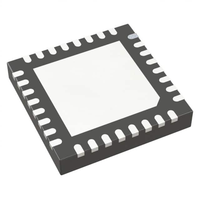
Analog Devices Inc. AD7124-4BCPZ
- Part No.:
- AD7124-4BCPZ
- Manufacturer:
- Analog Devices Inc.
- Category:
- Analog to Digital Converters (ADC)
- Package:
- 32-WFQFN Exposed Pad, CSP
- Datasheet:
-
 AD7124-4BCPZ.pdf
- Description:
- IC ADC 24BIT SIGMA-DELTA 32LFCSP
- Quantity:
- Payment:

- Shipping:

Inventory:474
Please send an inquiry. Send us your inquiry, and we will respond immediately.
Product details
Overview
AD7124-4BCPZ from Analog Devices is a 24-bit sigma-delta ADC with integrated PGA, reference, excitation currents, and diagnostics-designed for high-precision sensor measurement. It supports 4 differential or 7 pseudo-differential inputs, offers three power modes (255 µA/355 µA/930 µA typical), delivers 24 nV rms noise at 1.17 SPS (gain = 128), and operates across −40°C to +125°C in a 32-lead LFCSP package.
For engineers reviewing the AD7124-4BCPZ datasheet, AD7124-4BCPZ pinout, AD7124-4BCPZ application, or AD7124-4BCPZ equivalent, key selection criteria include simultaneous 50/60 Hz rejection at 25 SPS, per-channel configuration support, internal 10 ppm/°C reference drift, rail-to-rail analog input capability for gains > 1, and integrated diagnostics enabling SIL-certifiable system design.
Technical Context
The AD7124-4BCPZ implements a multi-stage sigma-delta modulator with programmable sinc4/sinc3/fast-settling/post filters, enabling configurable trade-offs between noise, settling time, and 50/60 Hz rejection. Its on-chip PGA (gain 1–128) and matched excitation current sources (0.1–1000 µA) allow direct interface to RTDs, thermocouples, and bridge sensors without external signal conditioning.
Diagnostics include CRC-protected register access, reference detect, power supply monitoring (ALDO/DLDO), AIN over/undervoltage detection, burnout current control, and temperature sensor readback-all coordinated via an automatic channel sequencer supporting up to 16 channels (analog + diagnostic). The device uses either internal 614.4 kHz oscillator or external clock, with SPI/QSPI/MICROWIRE-compatible 3-/4-wire serial interface and Schmitt-triggered SCLK.
Key Specifications
| Parameter | Value and Actual Design Meaning |
|---|---|
| Resolution | 24-bit no missing codes; supports up to 22 noise-free bits at gain = 1 |
| Output Data Rate Range | 1.17–19,200 SPS across low/mid/full power modes-enables flexible scan rate vs. power trade-off |
| RMS Noise (gain = 128) | 24 nV (low power), 20 nV (mid power), 23 nV (full power)-directly determines minimum resolvable sensor change |
| Reference Drift | 10 ppm/°C max (LFCSP package)-ensures stable full-scale accuracy over industrial temperature range |
| Common-Mode Rejection | 115 dB min at gain ≥ 8-rejects interference in noisy industrial environments |
| Power Supply Rejection | 99 dB (full power mode, gain = 1 or >16)-minimizes error from AVDD ripple or coupling |
| Diagnostic Coverage | SIL-compliant features including CRC, signal chain check, reference detect, and LDO monitoring-reduces external safety circuitry |
Pinout & Package
AD7124-4BCPZ is housed in a 32-lead, 5 mm × 5 mm × 0.75 mm LFCSP package with exposed thermal pad. Pin functions are validated per Analog Devices AD7124-4 Rev. E datasheet (pages 15–17).
| Pin/Terminal | Circuit Role | Design Meaning |
|---|---|---|
| AVDD, AVSS | Analog supply rails | Support 2.7–3.6 V single supply or ±1.8 V dual supply; AVSS may be negative for bipolar operation |
| IOVDD | Digital interface supply | Independent 1.65–3.6 V rail enables level-shifting with host MCU I/O |
| AIN0–AIN3 | Differential analog inputs | Configurable as 4 differential or 7 pseudo-differential channels; support rail-to-rail input for gains > 1 |
| REFIN+, REFIN− | Reference input terminals | Accept external differential reference (0.5–AVDD V); internal reference buffered or unbuffered |
| DOUT/RDY | Data output / ready indicator | Open-drain RDY signal asserts when conversion data is ready; also serves as serial data output |
| SCLK, CS, DIN | Serial interface signals | 3-/4-wire SPI-compatible interface with Schmitt-triggered SCLK for noise immunity |
| P1, P2 | General-purpose outputs | Programmable logic outputs usable for sensor enable, multiplexer control, or status indication |
| VBIAS | Bias voltage generator output | Provides AVDD/2 common-mode voltage to analog inputs-eliminates need for external bias network |
| IOUT0, IOUT1 | Excitation current sources | Matched, programmable (0.1–1000 µA) current sinks usable for RTD/bridge excitation |
| SYNC | Conversion synchronization | External trigger for synchronized sampling across multiple ADCs or with external events |
Key Features
| Feature | Design Value |
|---|---|
| Three selectable power modes | Enables optimization of current consumption (255–930 µA) vs. noise (20–24 nV rms) and data rate (1.17–19.2 kSPS) |
| Simultaneous 50 Hz/60 Hz rejection | 80+ dB rejection at 25 SPS with single-cycle settling-critical for AC-line-noise-prone industrial sites |
| Per-channel configuration registers | Eight independent setups (gain, filter, ODR, reference, buffering) assignable per input-supports mixed-sensor systems |
| Integrated diagnostics suite | CRC, reference detect, power monitor, burnout detection, and memory checksum-reduces external components and validation effort |
| On-chip bias voltage generator | Delivers precise AVDD/2 common-mode voltage directly to AIN pins-removes external resistor divider and op amp |
| Low-side power switch | 7–10 Ω RON switch enables bridge sensor power-down between conversions-cuts system standby power |
Applications
| Temperature Measurement | Pressure Measurement |
|---|---|
Use Scenario: High-accuracy RTD or thermocouple readout in process transmitters with ambient temperature ranging from −40°C to +85°C. IC Role / Device Role / Timing Role: Primary ADC front end performing cold-junction compensation, linearization, and digital filtering before sending calibrated data to MCU. Use Value: 24-bit resolution and 20 nV rms noise enable <0.01°C RTD resolution; internal reference drift ≤10 ppm/°C ensures long-term stability without recalibration. | Use Scenario: Strain-gauge-based pressure sensor in hydraulic control systems requiring functional safety compliance (IEC 61508). IC Role / Device Role / Timing Role: Signal conditioner and converter for Wheatstone bridge output, with excitation current sourcing and burnout detection. Use Value: Matched 0.1–1000 µA excitation currents and 115 dB CMRR suppress bridge imbalance errors; integrated diagnostics achieve >90% safe failure fraction (SFF). |
| Industrial Process Control | Smart Transmitters |
Use Scenario: Multi-sensor field instrument measuring flow, level, and temperature simultaneously in hazardous area enclosures. IC Role / Device Role / Timing Role: Central analog acquisition hub managing up to 16 channels (including diagnostics) via automatic sequencer. Use Value: Per-channel configuration allows independent ODR/filter/gain settings-e.g., fast 19.2 kSPS for vibration, slow 25 SPS for temperature-with single-device coordination. | Use Scenario: HART-enabled 4–20 mA smart transmitter with local display and wireless telemetry, operating on loop power. IC Role / Device Role / Timing Role: Low-power precision ADC subsystem minimizing total active current while maintaining 22-bit noise-free resolution. Use Value: 255 µA typical current in low power mode extends battery life; power-down current ≤3 µA enables ultra-low-quiescent sleep states. |
Equivalent & Alternatives
The following parts are listed as comparable options for similar high-precision sigma-delta ADC applications.
| Alternative Part | Technical Difference | Application Difference | Selection Advice |
|---|---|---|---|
| AD7124-8BCPZ | 8-channel variant (vs. 4-channel); identical architecture, specs, and package; higher pin count (40-lead LFCSP) | Requires PCB redesign due to different pinout and package; suitable only when additional analog inputs are needed | Select when expanding channel count without changing signal chain architecture or calibration methodology |
| LTC2499CGN#PBF | 24-bit delta-sigma ADC with 16-channel mux; no integrated PGA, reference, or excitation currents; higher noise (35 nV rms) | Lacks on-chip diagnostics, bias generator, and sensor excitation-requires external components for RTD/bridge use | Choose for cost-sensitive, lower-precision applications where external signal conditioning is acceptable |
Compared with AD7124-8BCPZ, the AD7124-4BCPZ saves board space and BOM cost in 4-channel systems; compared with LTC2499CGN#PBF, it reduces design complexity and improves system-level accuracy by integrating PGA, reference, excitation, and diagnostics-making it optimal for certified industrial transmitters.
Availability
AD7124-4BCPZ is available at Aetrix Electronics and suitable for industrial process control, smart transmitter development, and high-reliability temperature/pressure measurement requiring stable component supply across extended temperature ranges and long production lifecycles.
Supply support for AD7124-4BCPZ includes scheduled delivery planning, volume procurement assistance, BOM continuity management, traceable sourcing, and lifecycle availability coordination for OEM customers, industrial embedded developers, connected-device designers, and electronics production programs.
Manufacturer
Analog Devices is a global leader in high-performance analog, mixed-signal, and digital signal processing semiconductors, serving industrial, automotive, communications, and healthcare markets since 1965.
The AD7124 family was designed specifically for high-precision, low-power sensor measurement in harsh industrial environments-integrating signal conditioning, conversion, diagnostics, and power management into a single IC to simplify certified system design.
FAQ
What is the maximum output data rate of the AD7124-4BCPZ in full power mode?
The AD7124-4BCPZ supports a maximum output data rate of 19,200 SPS in full power mode. This rate is achievable with sinc3 or sinc4 filters and enables high-speed applications such as vibration monitoring or fast-loop control. At this rate, RMS noise increases to 23 nV rms (gain = 128), and current consumption rises to 930 µA typical. Filter selection and ODR must be configured via the ADC_CONTROL and FILTER registers.
Does the AD7124-4BCPZ include an internal voltage reference, and what is its accuracy?
Yes, the AD7124-4BCPZ integrates a precision band gap reference with 2.5 V nominal output, ±0.2% initial accuracy at 25°C, and maximum drift of 10 ppm/°C over −40°C to +125°C (LFCSP package). It supplies 70 µA and features 85 dB PSR. The reference can be used internally or buffered for external circuits. External references (0.5–AVDD V) are also supported with buffered/unbuffered options.
How many analog input channels does the AD7124-4BCPZ support, and how are they configured?
The AD7124-4BCPZ supports up to four fully differential analog inputs (AIN0–AIN3) or seven pseudo-differential inputs using shared AINx pins. Configuration is done per channel via eight independent setup registers, each defining gain (1–128), filter type, output data rate, buffering, and reference source. The automatic channel sequencer manages conversions across enabled channels-including diagnostics-without host intervention.
What diagnostic functions are built into the AD7124-4BCPZ, and how do they support functional safety?
The AD7124-4BCPZ includes CRC-protected register access, reference detect, power supply monitors (ALDO/DLDO), AIN over/undervoltage detection, burnout current control, and memory checksums. These features collectively enable >90% safe failure fraction (SFF) per IEC 61508. Diagnostics run autonomously or on-demand, reducing software validation burden and eliminating need for external watchdogs or reference buffers in SIL2-capable designs.
What package type and thermal characteristics apply to the AD7124-4BCPZ?
The AD7124-4BCPZ is supplied in a 32-lead LFCSP package (5 mm × 5 mm × 0.75 mm) with exposed thermal pad. Its thermal resistance θJA is 36°C/W (JEDEC standard board), and θJC is 5.5°C/W. The package supports −40°C to +125°C operation and is RoHS-compliant. Pin compatibility with AD7124-4 variants is maintained within the same package family, but AD7124-4BCPZ is not pin-compatible with the TSSOP version.
AD7124-4BCPZ Specifications
- Product attributes
- Attribute value
- Manufacturer:
- Analog Devices Inc.
- Series:
- -
- Package/Case:
- 32-WFQFN Exposed Pad, CSP
- Packaging:
- Tray
- Product Status:
- Active
- Number of Bits:
- 24
- Sampling Rate (Per Second):
- 19.2k
- Number of Inputs:
- 4, 7
- Input Type:
- Differential, Single Ended
- Data Interface:
- SPI
- Configuration:
- MUX-PGA-ADC
- Ratio - S/H:ADC:
- -
- Number of A/D Converters:
- 1
- Architecture:
- Sigma-Delta
- Reference Type:
- External, Internal
- Voltage - Supply, Analog:
- ±1.8V, 2.7V ~ 3.6V
- Voltage - Supply, Digital:
- 1.65V ~ 3.6V
- Features:
- PGA, Temperature Sensor
- Operating Temperature:
- -40°C ~ 105°C
- Supplier Device Package:
- 32-LFCSP (5x5)
- Mounting Type:
- Surface Mount
- Grade:
- -
- Qualification:
- -
AD7124-4BCPZ FAQ
1.How can I place an order for AD7124-4BCPZ through Aetrix?
Please submit a Request for Quotation (RFQ) for AD7124-4BCPZ on Aetrix. Our sales agent will provide a competitive quotation and guide you through the order confirmation once you accept the terms.
2.Are the price and stock information for AD7124-4BCPZ reliable?
The price and inventory of AD7124-4BCPZ are updated periodically and may fluctuate due to market conditions. Stock and pricing data are typically refreshed every 24 hours. Quotation validity for AD7124-4BCPZ is usually 5 days.
3.What payment methods are accepted for AD7124-4BCPZ?
We accept Wire Transfer, PayPal, Credit Card, Western Union, MoneyGram, and Escrow for AD7124-4BCPZ transactions.
Note: Certain payment methods may incur a processing fee.
4.How is shipping managed for AD7124-4BCPZ?
AD7124-4BCPZ orders can be shipped via leading logistics carriers, including DHL, UPS, FedEx, TNT, or Registered Mail.
Once your AD7124-4BCPZ order is processed, you will receive an email with the shipment details and tracking number.
Note: Tracking information may take up to 24 hours to appear. Express delivery typically takes 3–5 business days.
5.How can I obtain technical support or documentation for AD7124-4BCPZ?
For technical support, including AD7124-4BCPZ datasheets, pinout diagrams, or application guidance, please contact our engineering support team. They can provide detailed documentation and assistance for your AD7124-4BCPZ requirements.
6.How does Aetrix verify that AD7124-4BCPZ is sourced from the original manufacturer or authorized distributors?
All AD7124-4BCPZ products on Aetrix are procured from qualified distributors and authorized channels. Our dedicated quality assurance team conducts strict verification, including traceability checks and, if necessary, third-party testing. This ensures that AD7124-4BCPZ meets industry standards.
7.What is the process for return or replacement of AD7124-4BCPZ?
All AD7124-4BCPZ units undergo pre-shipment inspection (PSI). If there is an issue with AD7124-4BCPZ, returns or replacements are accepted under the following conditions:
1.Quantity discrepancies, incorrect items, or visible external defects (such as breakage or corrosion), acknowledged by Aetrix.
2.The issue is reported within 90 days of delivery.
3.The AD7124-4BCPZ part is unused and in its original packaging.
Return procedure for AD7124-4BCPZ:
1.Submit a request within 90 days.
2.Obtain a Return Material Authorization (RMA) from Aetrix.
AD7124-4BCPZ Tags
-
ADC081C021CIMKX/NOPB
Texas Instruments

-
MCP3021A5T-E/OT
Microchip Technology
-
TLA2024IRUGR
Texas Instruments
-
MCP3221A5T-E/OT
Microchip Technology
-
MCP3221A5T-I/OT
Microchip Technology
-
MCP3221A4T-E/OT
Microchip Technology
-
MCP3221A6T-E/OT
Microchip Technology
-
MCP3221A0T-E/OT
Microchip Technology
-
MCP3221A1T-E/OT
Microchip Technology

-
ADC121S021CIMFX/NOPB
Texas Instruments

-
MCP3001-I/MS
Microchip Technology

-
MCP3001-I/SN
Microchip Technology
Tech Hub

A practical engineering guide to 3.3V and 5V logic compatibility, input thresholds, resistor dividers, translator ICs, MOSFET level shifting, I2C pull-ups, timing limits and power-sequencing risks.

The 74HC595 uses push-pull logic outputs, while the TPIC6B595 uses 50 V open-drain DMOS sinks for higher-power loads. This guide compares timing, current limits, 3.3 V interfacing, load wiring, thermal…

The 74HC595 converts serial data into eight stable parallel outputs. This guide covers pin functions, shift and storage timing, OE and MR behavior, drive-current limits, cascading, voltage compatibilit…

A technical comparison of level-sensitive latches and edge-triggered flip-flops, covering timing windows, setup and hold limits, master–slave operation, time borrowing, race-through, HDL inference and…

A D latch stores one bit while Enable controls when data can pass. This reference covers gate-level operation, truth tables, transparency, setup and hold timing, LE versus OE, common ICs and practical …

An SR latch stores one bit through cross-coupled feedback. This engineering reference covers NOR and NAND implementations, truth tables, forbidden-state recovery, gated operation, switch debouncing, fa…

Latch circuits retain one bit through feedback. This technical reference covers SR and D latches, truth tables, transparency, timing limits, latch-versus-flip-flop behavior, applications and common log…

An engineering guide to LED driver operation, constant-current and constant-voltage outputs, linear and switching topologies, dimming, IC selection, calculations, replacement compatibility, and fault c…

Operational amplifier guide covering op amp basics, feedback, ideal vs real op amps, common configurations, buffer circuits, offset, bias current, gain-bandwidth, slew rate, rail-to-rail limits and sel…

Jumper cables guide covering safe connection order, red and black clamp placement, final ground connection, cable gauge, length, clamp quality, copper vs CCA cables, jump starter comparison and battery…


