
 My Inquiry
 My Account


Analog Devices Inc. AD7341JP
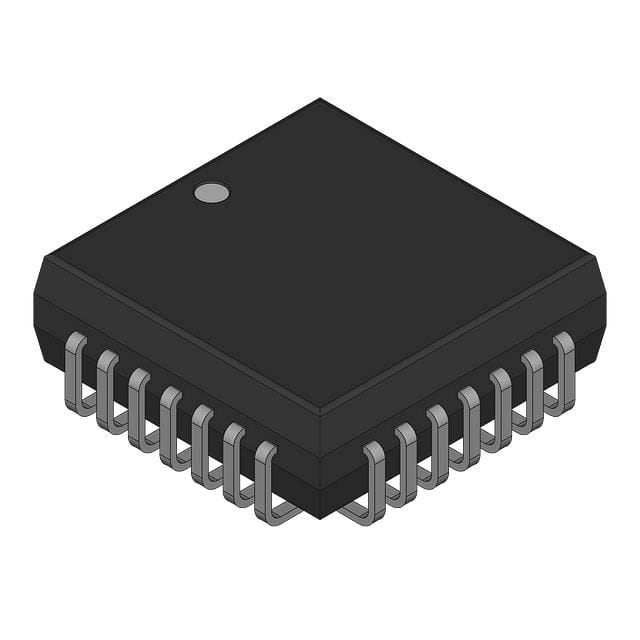
- Part No.:
- AD7341JP
- Manufacturer:
- Analog Devices Inc.
- Category:
- Specialized ICs
- Package:
- 28-LCC (J-Lead)
- Datasheet:
-
 AD7341JP.pdf
- Description:
- IC DIGITALLY PROG FILTER 28PLCC
- Quantity:
- Payment:

- Shipping:

Inventory:1,820
Please send an inquiry. Send us your inquiry, and we will respond immediately.
Product details
Overview
AD7341JP from Analog Devices is a voiceband reconstruction filter IC designed for the transmit path of high-speed CCITT V.32/V.33 modems, implementing a seventh-order switched-capacitor low-pass + second-order continuous-time low-pass architecture with 3.5 kHz cutoff, programmable 0 dB to –38 dB attenuation (6-bit digital control), and 75 dB SNR at 1 kHz. It interfaces directly with 14-bit DACs like the AD7840 in analog front-end signal chains.
For engineers reviewing the AD7341JP datasheet, AD7341JP pinout, AD7341JP application, or AD7341JP equivalent, this device is selected for precise transmit-channel spectral shaping in echo-cancelling modem designs requiring stable group delay, <0.4 dB passband ripple (0–3.3 kHz), and >70 dB stopband rejection above 6.1 kHz.
Technical Context
The AD7341JP uses a dual-stage filtering architecture: a fully differential seventh-order elliptical switched-capacitor low-pass filter (SCF) clocked at 57.6 kHz (derived from 288 kHz CLKIN via ×5 divider), followed by a second-order continuous-time low-pass smoothing stage. Its cutoff frequency is fixed at 3.5 kHz (0.1 dB down point) and exhibits <2% unit-to-unit variation due to capacitor matching.
Digital control includes WR-latched 6-bit attenuation programming (DB2–DB7), asynchronous SYNCIN for SCF clock alignment, and programmable input/output dividers (DPO/DPI, DSO/DS1/DS2) enabling synchronized timing with external DACs - critical for avoiding low-frequency aliasing in 9.6 kHz or 7.2 kHz sampling systems.
Key Specifications
| Parameter | Value and Actual Design Meaning |
|---|---|
| Cutoff Frequency | 3.5 kHz - 0.1 dB down point; defines maximum usable voiceband transmit bandwidth per V.32/V.33. |
| Attenuation Range | 0 dB to –38 dB - digitally programmable via DB2–DB7; enables line-level adaptation across global PSTN standards. |
| Signal-to-Noise Ratio | 75 dB typ - measured over 0–3.5 kHz with 1 kHz sine input; ensures clean reconstruction before line driver stage. |
| Stopband Rejection | 70 dB min above 6.1 kHz - suppresses aliasing artifacts from DAC output imaging. |
| Passband Ripple | 0.4 dB max (0–3.3 kHz) - preserves amplitude fidelity of voiceband tones and signaling frequencies. |
| Supply Voltages | ±5 V (±5%) on VDD/VCC (+5 V), VSS (–5 V); AGND/DGND isolated - supports mixed-signal integrity in modem AFEs. |
| CLKIN Frequency | 288 kHz (default), scalable to 576/864/1152 kHz via NI = 1–4 - allows flexible system clock sourcing while maintaining 57.6 kHz SCF clock. |
Pinout & Package
AD7341JP is housed in a 28-pin Plastic Leaded Chip Carrier (PLCC) package with gull-wing leads, rated for 0°C to +70°C operation (J-grade). Pin 1 identifier is marked by a notch or dot; thermal pad is not electrically connected.
| Pin/Terminal | Circuit Role | Design Meaning |
|---|---|---|
| TXIN (Pin 24) | Analog Input | Differential-conversion input for DAC output; accepts ±3 V signal range. |
| TXOUT (Pin 1) | Analog Output | Single-ended filtered output; drives line interface amplifier with 0.2 Ω output impedance. |
| VDD (Pin 23), VCC (Pin 8), VSS (Pin 2) | Power Supplies | VDD/VCC = +5 V (analog/digital), VSS = –5 V; independent AGND (Pin 22) and DGND (Pin 7) required. |
| WR (Pin 13) | Digital Control | Active-low latch enable for DB2–DB7 attenuation code; edge-triggered write timing (tWR ≥ 80 ns). |
| DB2–DB7 (Pins 14–19) | Digital Input Bus | 6-bit parallel bus setting attenuation level (0–38 dB in 6 dB steps); latched on WR rising edge. |
| CLKIN (Pin 12) | Clock Input | Primary clock source (288 kHz default); internally divided by 5 to generate 57.6 kHz SCF clock. |
| SYNCOUT (Pin 3) | Synchronization Output | Derived from SCF clock (fCLKIN/(N1×5×N2)); used to drive DAC LDAC or system timing logic. |
| SYNCIN (Pin 9) | Asynchronous Reset | Resets internal SYNCOUT divider counter; enables cycle-slipping for precise sampling phase alignment. |
| DPO/DPI (Pins 11/10), DSO/DS1/DS2 (Pins 4/5/6) | Programmable Dividers | Set N1 (1–4) and N2 (1–8) to configure CLKIN and SYNCOUT frequencies independently. |
Key Features
| Feature | Design Value |
|---|---|
| CCITT V.32/V.33 Compliance | Guaranteed passband (0–3.3 kHz), group delay flatness, and stopband rejection meet full V.32/V.33 analog front-end requirements. |
| Differential Switched-Capacitor Architecture | Reduces clock feedthrough to –65 dB (typ), improving harmonic distortion (<–80 dB THD) and common-mode noise immunity. |
| Integrated Clock Generation | On-chip programmable dividers eliminate need for external clock synthesizers; supports multiple master clock frequencies. |
| Programmable Attenuation Accuracy | ±0.1 dB relative accuracy over full 0–38 dB range - enables precise line-level calibration without external trim. |
| Low Group Delay Variation | ≤350 µs differential group delay (0–3.3 kHz, referenced to 1 kHz) - preserves phase coherence of multi-tone signals. |
Applications
| Voiceband Modem Transmit Path | Echo-Canceling Modem AFE |
|---|---|
|
Use Scenario: Transmit-side signal conditioning in V.32/V.33 full-duplex modems operating at 14.4 kbps. IC Role / Device Role / Timing Role: Reconstruction filter placed between 14-bit DAC (e.g., AD7840) and line driver; shapes spectrum and removes imaging artifacts. Use Value: Enables compliance with ITU spectral masks and minimizes inter-symbol interference through precise 3.5 kHz cutoff and <0.4 dB ripple. |
Use Scenario: Analog front-end in DSP-based echo-cancellation modems using ADSP-2101 or similar. IC Role / Device Role / Timing Role: Provides synchronized, low-jitter transmit path timing via SYNCOUT to coordinate DAC updates and ADC sampling. Use Value: Eliminates low-frequency aliasing by ensuring SCF clock (57.6 kHz) is integer-multiple of DAC update rate (e.g., 9.6 kHz). |
| Global PSTN Line Interface | Telecom Data Pump Design |
|
Use Scenario: Adapting modem output to regional line impedance and loss profiles (e.g., North America vs. Europe). IC Role / Device Role / Timing Role: Programmable attenuation stage (0 to –38 dB) calibrated via DB2–DB7 to match local loop gain requirements. Use Value: Avoids external attenuator networks; maintains SNR integrity while meeting regulatory line-level limits (e.g., –6 dBm to –12 dBm). |
Use Scenario: High-fidelity data pump implementation in embedded telecom gateways or fax servers. IC Role / Device Role / Timing Role: Low-distortion reconstruction filter preserving spectral purity of multi-carrier (QAM) symbols. Use Value: Delivers >75 dB SNR and <–80 dB harmonic distortion - essential for maintaining BER <10⁻⁶ under noisy line conditions. |
Equivalent & Alternatives
The following parts are listed as comparable options for similar voiceband reconstruction filter applications.
| Alternative Part | Technical Difference | Application Difference | Selection Advice |
|---|---|---|---|
| AD7341JN | Same silicon, 24-pin PDIP package; identical electrical specs but larger footprint and no PLCC thermal performance. | Preferred for prototyping or through-hole PCBs; lacks PLCC's compact size and gull-wing solder reliability. | Select AD7341JN only when PLCC assembly infrastructure is unavailable or manual rework is required. |
| MAX274ACPP+ | Continuous-time 8th-order LPF; no digital attenuation; fixed 3.4 kHz cutoff; single +5 V supply. | Requires external PGA for level control; unsuitable for V.33-compliant systems needing programmable attenuation. | Choose MAX274ACPP+ only for cost-sensitive, non-V.32/V.33 designs where digital control and dual-supply operation are unnecessary. |
Compared with AD7341JN and MAX274ACPP+, the AD7341JP uniquely combines PLCC packaging, integrated 6-bit programmable attenuation, and guaranteed V.32/V.33 compliance - making it the only drop-in solution for production modem AFEs requiring both compact layout and field-updatable line calibration.
Availability
AD7341JP is available at Aetrix Electronics and suitable for voiceband modem design, telecom data pump development, and echo-cancelling AFE integration requiring stable component supply across industrial temperature ranges and long product lifecycles.
Supply support for AD7341JP includes scheduled delivery planning, volume procurement assistance, BOM continuity management, traceable sourcing, and lifecycle availability coordination for OEM customers, industrial embedded developers, connected-device designers, and electronics production programs.
Manufacturer
Analog Devices is a global leader in high-performance analog, mixed-signal, and digital signal processing semiconductors, founded in 1965 and headquartered in Wilmington, MA.
The AD7341JP belongs to Analog Devices' LC2MOS voiceband filter family, engineered specifically for CCITT V.32/V.33 modem analog front-ends - emphasizing low distortion, precise cutoff control, and seamless digital interfacing with 14-bit DACs.
FAQ
What is the primary function of the AD7341JP in a modem system?
The AD7341JP serves as the transmit reconstruction filter in CCITT V.32/V.33 modems, smoothing the stepped output of a 14-bit DAC (e.g., AD7840) into a band-limited analog signal. Its 3.5 kHz cutoff, programmable attenuation, and low group delay ensure compliance with international spectral masks and minimize inter-symbol interference - critical for reliable 14.4 kbps operation. The AD7341JP achieves this using a hybrid switched-capacitor + continuous-time architecture.
How does the AD7341JP achieve synchronization with external DACs?
The AD7341JP generates a synchronized clock on-chip via its SYNCOUT pin, derived from the internal 57.6 kHz switched-capacitor filter clock (fCLKIN/(N1×5×N2)). By configuring DSO/DS1/DS2, users set N2 to produce exact integer multiples of standard DAC update rates (e.g., 9.6 kHz or 7.2 kHz). This eliminates low-frequency aliasing. The SYNCIN pin further enables cycle-slipping for sub-cycle phase alignment - a capability built into the AD7341JP's clock generation circuitry.
What are the supply voltage requirements for the AD7341JP?
The AD7341JP requires three independent supplies: VDD = +5 V (±5%) for analog circuitry, VCC = +5 V (±5%) for digital logic, and VSS = –5 V (±5%) for analog biasing. AGND (Pin 22) and DGND (Pin 7) must be kept separate and tied to their respective supply returns. This triple-supply, split-ground architecture ensures >75 dB SNR and <–80 dB harmonic distortion - key specifications verified in the AD7341JP datasheet under these exact conditions.
Can the AD7341JP be used with clock frequencies other than 288 kHz?
Yes - the AD7341JP supports CLKIN frequencies of 288 kHz, 576 kHz, 864 kHz, or 1.152 MHz via programmable input divider (N1 = 1–4 set by DPO/DPI). Regardless of input frequency, the internal SCF clock remains fixed at 57.6 kHz because the divider always applies a ×5 factor. This flexibility allows system designers to use common clock sources while guaranteeing consistent filter response - a feature explicitly documented for the AD7341JP in Analog Devices' datasheet Rev. A.
What is the significance of the 0.1 dB cutoff definition for the AD7341JP?
The AD7341JP's cutoff frequency is defined as the point where gain drops 0.1 dB from the lowest passband level - not the conventional –3 dB point. This stringent definition ensures minimal amplitude deviation across the entire 0–3.3 kHz voiceband, directly supporting CCITT V.32/V.33 requirements for tone transmission fidelity and signaling accuracy. Measured passband ripple is ≤0.4 dB within this band, confirming the AD7341JP's suitability for high-SNR modem applications.
AD7341JP Specifications
- Product attributes
- Attribute value
- Manufacturer:
- Analog Devices Inc.
- Series:
- AD7341
- Package/Case:
- 28-LCC (J-Lead)
- Packaging:
- Bulk
- Product Status:
- Active
- Programmable:
- Not Verified
- Type:
- Voiceband Reconstruction, Antialiasing Filter Set
- Applications:
- -
- Mounting Type:
- Surface Mount
- Supplier Device Package:
- 28-PLCC (11.51x11.51)
- Grade:
- -
- Qualification:
- -
AD7341JP FAQ
1.How can I place an order for AD7341JP through Aetrix?
Please submit a Request for Quotation (RFQ) for AD7341JP on Aetrix. Our sales agent will provide a competitive quotation and guide you through the order confirmation once you accept the terms.
2.Are the price and stock information for AD7341JP reliable?
The price and inventory of AD7341JP are updated periodically and may fluctuate due to market conditions. Stock and pricing data are typically refreshed every 24 hours. Quotation validity for AD7341JP is usually 5 days.
3.What payment methods are accepted for AD7341JP?
We accept Wire Transfer, PayPal, Credit Card, Western Union, MoneyGram, and Escrow for AD7341JP transactions.
Note: Certain payment methods may incur a processing fee.
4.How is shipping managed for AD7341JP?
AD7341JP orders can be shipped via leading logistics carriers, including DHL, UPS, FedEx, TNT, or Registered Mail.
Once your AD7341JP order is processed, you will receive an email with the shipment details and tracking number.
Note: Tracking information may take up to 24 hours to appear. Express delivery typically takes 3–5 business days.
5.How can I obtain technical support or documentation for AD7341JP?
For technical support, including AD7341JP datasheets, pinout diagrams, or application guidance, please contact our engineering support team. They can provide detailed documentation and assistance for your AD7341JP requirements.
6.How does Aetrix verify that AD7341JP is sourced from the original manufacturer or authorized distributors?
All AD7341JP products on Aetrix are procured from qualified distributors and authorized channels. Our dedicated quality assurance team conducts strict verification, including traceability checks and, if necessary, third-party testing. This ensures that AD7341JP meets industry standards.
7.What is the process for return or replacement of AD7341JP?
All AD7341JP units undergo pre-shipment inspection (PSI). If there is an issue with AD7341JP, returns or replacements are accepted under the following conditions:
1.Quantity discrepancies, incorrect items, or visible external defects (such as breakage or corrosion), acknowledged by Aetrix.
2.The issue is reported within 90 days of delivery.
3.The AD7341JP part is unused and in its original packaging.
Return procedure for AD7341JP:
1.Submit a request within 90 days.
2.Obtain a Return Material Authorization (RMA) from Aetrix.
AD7341JP Tags

-
CAP200DG-TL
Power Integrations
-
ATSHA204A-MAHDA-T
Microchip Technology

-
ATSHA204A-SSHDA-T
Microchip Technology

-
ATSHA204A-STUCZ-T
Microchip Technology
-
ATECC608B-MAHDA-T
Microchip Technology
-
ATECC608B-MAHCZ-S
Microchip Technology

-
ATECC608B-SSHDA-T
Microchip Technology
-
ATECC608B-MAHDA-S
Microchip Technology
-
ATECC608A-MAHDA-S
Microchip Technology
-
ATECC608B-MAVDA-T
Microchip Technology

-
ATECC608A-SSHDA-T
Microchip Technology
-
ATECC508A-MAHDA-T
Microchip Technology
Tech Hub

A practical engineering guide to 3.3V and 5V logic compatibility, input thresholds, resistor dividers, translator ICs, MOSFET level shifting, I2C pull-ups, timing limits and power-sequencing risks.

The 74HC595 uses push-pull logic outputs, while the TPIC6B595 uses 50 V open-drain DMOS sinks for higher-power loads. This guide compares timing, current limits, 3.3 V interfacing, load wiring, thermal…

The 74HC595 converts serial data into eight stable parallel outputs. This guide covers pin functions, shift and storage timing, OE and MR behavior, drive-current limits, cascading, voltage compatibilit…

A technical comparison of level-sensitive latches and edge-triggered flip-flops, covering timing windows, setup and hold limits, master–slave operation, time borrowing, race-through, HDL inference and…

A D latch stores one bit while Enable controls when data can pass. This reference covers gate-level operation, truth tables, transparency, setup and hold timing, LE versus OE, common ICs and practical …

An SR latch stores one bit through cross-coupled feedback. This engineering reference covers NOR and NAND implementations, truth tables, forbidden-state recovery, gated operation, switch debouncing, fa…

Latch circuits retain one bit through feedback. This technical reference covers SR and D latches, truth tables, transparency, timing limits, latch-versus-flip-flop behavior, applications and common log…

An engineering guide to LED driver operation, constant-current and constant-voltage outputs, linear and switching topologies, dimming, IC selection, calculations, replacement compatibility, and fault c…

Operational amplifier guide covering op amp basics, feedback, ideal vs real op amps, common configurations, buffer circuits, offset, bias current, gain-bandwidth, slew rate, rail-to-rail limits and sel…

Jumper cables guide covering safe connection order, red and black clamp placement, final ground connection, cable gauge, length, clamp quality, copper vs CCA cables, jump starter comparison and battery…


