
 My Inquiry
 My Account


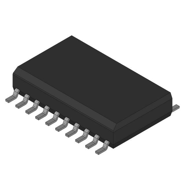
Analog Devices Inc. AD80052BR
- Part No.:
- AD80052BR
- Manufacturer:
- Analog Devices Inc.
- Category:
- Application Specific Clock/Timing
- Package:
- 20-SOIC (0.295", 7.50mm Width)
- Datasheet:
-
 AD80052BR.pdf
- Description:
- CLOCK RECOVERY AND DATA RETIMING
- Quantity:
- Payment:

- Shipping:

Inventory:1,923
Please send an inquiry. Send us your inquiry, and we will respond immediately.
Product details
Overview
AD80052BR from Analog Devices is a phase-locked loop (PLL) clock recovery and data retiming IC designed for NRZ serial data streams at 51.84 Mbps (STS-1). It performs frequency acquisition and phase lock without preamble or external VCXO, delivers differential recovered clock and retimed data outputs, and operates on single –5.2 V or +5 V supply across –40°C to +85°C.
For engineers reviewing the AD80052BR datasheet, AD80052BR pinout, AD80052BR application, or AD80052BR equivalent, key selection criteria include its 51.84 MHz nominal center frequency, 0.1% fractional loop bandwidth, ±20% VCO center-frequency tolerance in free-run mode, 0.08 dB jitter peaking at ζ = 5, and support for ECL-compatible differential I/O with 208° peak-to-peak random jitter performance.
Technical Context
The AD80052BR implements a second-order PLL architecture with dual control loops: a frequency detector enables rapid initial frequency acquisition, followed by a patented phase detector for precise phase lock. Its loop damping is user-programmable via external capacitor CD (0.15 µF nominal for ζ = 5), directly governing jitter peaking (0.08 dB) and acquisition time (4 × 10⁵ bit periods).
It accepts NRZ input without preamble, generates differential CLKOUT and DATAOUT signals referenced to analog/digital ground planes, and provides FRAC output pulses during frequency slip events-enabling lock-status monitoring. The integrated, trimmed VCO eliminates external tuning components and ensures ±20% center-frequency stability in absence of input data.
Key Specifications
| Parameter | Value and Actual Design Meaning |
|---|---|
| Nominal Center Frequency | 51.84 MHz - matches STS-1 telecom standard; defines VCO free-run frequency and PLL tracking range (49–53 Mbps). |
| Loop Bandwidth | 0.1% of center frequency (51.8 kHz) - sets jitter transfer cutoff and determines ability to track low-frequency input jitter. |
| Jitter Peaking | 0.08 dB at ζ = 5 - quantifies maximum gain in jitter transfer response; critical for minimizing amplified input jitter at loop resonance. |
| Acquisition Time | 4 × 10⁵ bit periods at ζ = 5 - time required to achieve frequency + phase lock from free-run state on random data. |
| Output Jitter | 2.5–4.7° rms (27–1 PRN) - measured phase noise on retimed data output; impacts system bit error rate under jittered input conditions. |
| Static Phase Error | 2–11.5° - steady-state phase offset between recovered clock edge and optimal data sampling point; affects timing margin. |
| Supply Voltage | –5.2 V (VEE) or +5 V (VCC) - single-rail operation compatible with ECL logic families; supports both negative- and positive-supply configurations. |
Pinout & Package
AD80052BR is housed in a 20-pin plastic SOIC package (R-20), 0.300" wide, with 1.27 mm pitch. Pin 1 is marked by bevelled corner; pins are arranged in two rows (1–10 top, 11–20 bottom), with dedicated analog/digital substrate and ground pins for noise isolation.
| Pin/Terminal | Circuit Role | Design Meaning |
|---|---|---|
| 1, 2 | DATAOUT | Differential retimed data output pair - requires 50 Ω termination; used to drive downstream ECL receivers with minimal skew. |
| 4, 5 | CLKOUT | Differential recovered clock output pair - provides low-jitter timing reference synchronized to input data transitions. |
| 16, 17 | DATAIN | Differential NRZ data input pair - accepts ECL-level signals; termination resistors must be placed adjacent to pins. |
| 19, 20 | FRAC | Differential frequency acquisition indicator - pulsed during cycle slips; used for lock-detection and system diagnostics. |
| 6, 7, 15 | VEE | Digital supply rail (–5.2 V or GND) - shared power return for digital circuitry; requires local 10 µF tantalum + 0.1 µF ceramic decoupling. |
| 9 | AVEE | Analog supply rail - isolated ground reference for VCO and phase detector; must be decoupled separately from digital VEE. |
| 11, 12 | CF1, CF2 | Loop damping capacitor inputs - connect to single external capacitor (0.15 µF for ζ = 5); sets PLL transient response and jitter peaking. |
Key Features
| Feature | Design Value |
|---|---|
| No preamble required | Enables lock acquisition on scrambled or random NRZ data - eliminates need for training sequences in telecom links. |
| Integrated trimmed VCO | Removes external tuning components and manual calibration - ensures ±20% center-frequency accuracy without adjustment. |
| Virtually eliminated pattern jitter | Patented phase detector suppresses jitter correlated to data transition density - maintains <0.5° jitter on 2⁷–1 PRN sequences. |
| Dual-loop acquisition | Frequency detector + phase detector architecture reduces total lock time vs. single-loop PLLs - achieves full lock in ≤400,000 bit periods. |
| Programmable damping | Single external capacitor selects damping factor (ζ = 1 to 10) - allows trade-off between acquisition speed (low ζ) and jitter peaking (high ζ). |
Applications
| SONET/SDH Line Card Timing | DS-3 to STS-1 Mapping Interface |
|---|---|
Use Scenario: Recovering clock and retiming data in OC-1 (STS-1) framer modules receiving scrambled T3 signals. IC Role / Device Role / Timing Role: Clock recovery and data retiming IC extracting 51.84 MHz clock from 51.84 Mbps NRZ input. Use Value: Eliminates need for external VCXO and preamble insertion, reducing BOM count and enabling seamless DS-3 to SONET mapping. | Use Scenario: Interfacing legacy DS-3 equipment (44.736 Mbps) with STS-1 transport layers (51.84 Mbps) in multiplexing gateways. IC Role / Device Role / Timing Role: Retiming device converting incoming DS-3 data to STS-1-aligned format using internal PLL lock. Use Value: Supports jitter-tolerant operation per OC-1 mask (Figure 12), ensuring BER <1×10⁻¹⁰ under specified input jitter profiles. |
| Telecom Test Equipment Data Recovery | ECL-Based Serial Link Repeater |
Use Scenario: Embedded in bit error rate testers (BERTs) to recover clock from stressed or jittered STS-1 signals during compliance validation. IC Role / Device Role / Timing Role: Reference clock generator and data resynchronizer providing clean, low-skew outputs for sampling circuits. Use Value: 0.2–0.6 ns recovered clock skew (tRCS) and 2.06–2.37 ns setup time enable precise edge alignment for high-speed sampling. | Use Scenario: Extending reach of ECL-based backplane serial links where signal integrity degrades over distance. IC Role / Device Role / Timing Role: Retiming repeater restoring jittered data and regenerating clean clock for downstream stages. Use Value: 208° peak-to-peak random jitter specification ensures minimal added jitter, preserving link timing budget. |
Equivalent & Alternatives
The following parts are listed as comparable options for similar clock recovery applications.
| Alternative Part | Technical Difference | Application Difference | Selection Advice |
|---|---|---|---|
| AD800-45BQ | 44.736 MHz center frequency; Cerdip package; 0°C to +70°C grade. | Targeted for DS-3 (44.736 Mbps) systems; lacks extended temperature range and SOIC packaging. | Select when operating in commercial temp range and requiring hermetic Cerdip reliability over plastic SOIC. |
| AD802-155BR | 155.52 MHz center frequency; 0.08% loop bandwidth; supports STS-3/STM-1 rates. | Designed for OC-3 (155.52 Mbps) applications; higher bandwidth increases sensitivity to high-frequency jitter. | Select for 155 Mbps systems; not suitable as direct replacement due to different center frequency and loop dynamics. |
Compared with AD800-45BQ and AD802-155BR, the AD80052BR offers optimized jitter peaking (0.08 dB) and acquisition time (4×10⁵ bits) specifically for STS-1, with industrial temperature support and SOIC packaging for cost-sensitive telecom line cards.
Availability
AD80052BR is available at Aetrix Electronics and suitable for SONET/SDH line card timing, DS-3 to STS-1 mapping interfaces, and telecom test equipment requiring stable component supply, long-term lifecycle support, and traceable sourcing.
Supply support for AD80052BR includes scheduled delivery planning, volume procurement assistance, BOM continuity management, traceable sourcing, and lifecycle availability coordination for OEM customers, industrial embedded developers, connected-device designers, and electronics production programs.
Manufacturer
Analog Devices is a global semiconductor company specializing in high-performance analog, mixed-signal, and digital signal processing technologies for precision instrumentation, communications, and industrial applications.
The AD800/AD802 product line was developed specifically for telecom clock recovery and data retiming in NRZ serial links, targeting STS-1, DS-3, and STM-1 standards with integrated VCOs and dual-loop PLL architectures.
FAQ
What is the nominal center frequency of the AD80052BR and how is it used?
The AD80052BR has a nominal center frequency of 51.84 MHz, matching the STS-1/OC-1 telecom standard. This value defines the VCO's free-run frequency and establishes the PLL's tracking and capture range (49–53 Mbps). During operation, the loop dynamically adjusts the VCO around this center to lock onto incoming NRZ data, making the AD80052BR suitable for STS-1 framer and mapping applications.
Does the AD80052BR require an external crystal or VCXO to operate?
No, the AD80052BR does not require an external crystal or VCXO. It integrates a precisely trimmed VCO that provides a clock output within ±20% of 51.84 MHz in the absence of input data. Lock acquisition relies solely on the internal frequency detector and phase detector, eliminating external timing components and simplifying board design for STS-1 clock recovery.
How is loop damping configured on the AD80052BR?
Loop damping on the AD80052BR is set using a single external capacitor connected between pins CF1 and CF2. A 0.15 µF capacitor yields a damping factor (ζ) of 5, resulting in 0.08 dB jitter peaking and 4 × 10⁵ bit-period acquisition time. Values can be adjusted to trade faster lock (lower ζ) against lower jitter peaking (higher ζ), with scaling governed by √(fDATA × CD).
What is the function of the FRAC output on the AD80052BR?
The FRAC (Frequency Acquisition) output on the AD80052BR is a differential signal that pulses during cycle slips between the input data and VCO frequencies. It indicates active frequency acquisition; pulses cease once frequency lock is achieved, signaling the start of phase acquisition. Engineers use FRAC to monitor lock status and synchronize downstream logic, as valid retimed data is guaranteed after the last FRAC pulse.
What supply voltage options does the AD80052BR support?
The AD80052BR supports single-supply operation at either –5.2 V (VEE) or +5 V (VCC), with all specifications guaranteed across –40°C to +85°C. The –5.2 V configuration uses ECL-compatible logic levels (VIH = –0.72 V, VOL = –1.60 V), while the +5 V mode requires level-shifting circuitry. Decoupling mandates a 10 µF tantalum capacitor on VEE/VCC and 0.1 µF ceramics on each power pin.
AD80052BR Specifications
- Product attributes
- Attribute value
- Manufacturer:
- Analog Devices Inc.
- Series:
- -
- Package/Case:
- 20-SOIC (0.295", 7.50mm Width)
- Packaging:
- Bulk
- Product Status:
- Active
- Programmable:
- Not Verified
- PLL:
- Yes
- Main Purpose:
- STS-1
- Input:
- ECL
- Output:
- ECL
- Number of Circuits:
- -
- Ratio - Input:Output:
- 1:2
- Differential - Input:Output:
- Yes/Yes
- Frequency - Max:
- 51.84MHz
- Voltage - Supply:
- 4.5V ~ 5.5V
- Operating Temperature:
- -40°C ~ 85°C
- Mounting Type:
- Surface Mount
- Grade:
- -
- Qualification:
- -
- Supplier Device Package:
- 20-SOIC
AD80052BR FAQ
1.How can I place an order for AD80052BR through Aetrix?
Please submit a Request for Quotation (RFQ) for AD80052BR on Aetrix. Our sales agent will provide a competitive quotation and guide you through the order confirmation once you accept the terms.
2.Are the price and stock information for AD80052BR reliable?
The price and inventory of AD80052BR are updated periodically and may fluctuate due to market conditions. Stock and pricing data are typically refreshed every 24 hours. Quotation validity for AD80052BR is usually 5 days.
3.What payment methods are accepted for AD80052BR?
We accept Wire Transfer, PayPal, Credit Card, Western Union, MoneyGram, and Escrow for AD80052BR transactions.
Note: Certain payment methods may incur a processing fee.
4.How is shipping managed for AD80052BR?
AD80052BR orders can be shipped via leading logistics carriers, including DHL, UPS, FedEx, TNT, or Registered Mail.
Once your AD80052BR order is processed, you will receive an email with the shipment details and tracking number.
Note: Tracking information may take up to 24 hours to appear. Express delivery typically takes 3–5 business days.
5.How can I obtain technical support or documentation for AD80052BR?
For technical support, including AD80052BR datasheets, pinout diagrams, or application guidance, please contact our engineering support team. They can provide detailed documentation and assistance for your AD80052BR requirements.
6.How does Aetrix verify that AD80052BR is sourced from the original manufacturer or authorized distributors?
All AD80052BR products on Aetrix are procured from qualified distributors and authorized channels. Our dedicated quality assurance team conducts strict verification, including traceability checks and, if necessary, third-party testing. This ensures that AD80052BR meets industry standards.
7.What is the process for return or replacement of AD80052BR?
All AD80052BR units undergo pre-shipment inspection (PSI). If there is an issue with AD80052BR, returns or replacements are accepted under the following conditions:
1.Quantity discrepancies, incorrect items, or visible external defects (such as breakage or corrosion), acknowledged by Aetrix.
2.The issue is reported within 90 days of delivery.
3.The AD80052BR part is unused and in its original packaging.
Return procedure for AD80052BR:
1.Submit a request within 90 days.
2.Obtain a Return Material Authorization (RMA) from Aetrix.
AD80052BR Tags
-
LMK00334RTVRQ1
Texas Instruments
.jpg)
-
DSC557-0344FI0T
Microchip Technology
-
9FGV0241AKILFT
Renesas

-
9DBL0452CKILFT
Renesas
-
DSC557-0344FL1T
Microchip Technology
-
RC19008AGND#KB0
Renesas
-
RC19008AGND#BB0
Renesas

-
9DB403DGILFT
Renesas
-
9DB233AGILFT
Renesas

-
9DB803DGILFT
Renesas
-
9FGL0851DKILFT
Renesas
-
AB-557-03-HCHC-F-L-C-T
Abracon LLC
Tech Hub

A practical engineering guide to 3.3V and 5V logic compatibility, input thresholds, resistor dividers, translator ICs, MOSFET level shifting, I2C pull-ups, timing limits and power-sequencing risks.

The 74HC595 uses push-pull logic outputs, while the TPIC6B595 uses 50 V open-drain DMOS sinks for higher-power loads. This guide compares timing, current limits, 3.3 V interfacing, load wiring, thermal…

The 74HC595 converts serial data into eight stable parallel outputs. This guide covers pin functions, shift and storage timing, OE and MR behavior, drive-current limits, cascading, voltage compatibilit…

A technical comparison of level-sensitive latches and edge-triggered flip-flops, covering timing windows, setup and hold limits, master–slave operation, time borrowing, race-through, HDL inference and…

A D latch stores one bit while Enable controls when data can pass. This reference covers gate-level operation, truth tables, transparency, setup and hold timing, LE versus OE, common ICs and practical …

An SR latch stores one bit through cross-coupled feedback. This engineering reference covers NOR and NAND implementations, truth tables, forbidden-state recovery, gated operation, switch debouncing, fa…

Latch circuits retain one bit through feedback. This technical reference covers SR and D latches, truth tables, transparency, timing limits, latch-versus-flip-flop behavior, applications and common log…

An engineering guide to LED driver operation, constant-current and constant-voltage outputs, linear and switching topologies, dimming, IC selection, calculations, replacement compatibility, and fault c…

Operational amplifier guide covering op amp basics, feedback, ideal vs real op amps, common configurations, buffer circuits, offset, bias current, gain-bandwidth, slew rate, rail-to-rail limits and sel…

Jumper cables guide covering safe connection order, red and black clamp placement, final ground connection, cable gauge, length, clamp quality, copper vs CCA cables, jump starter comparison and battery…


