
 My Inquiry
 My Account


Analog Devices Inc. AD8341ACPZ-WP
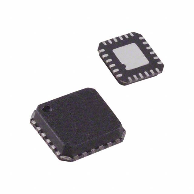
- Part No.:
- AD8341ACPZ-WP
- Manufacturer:
- Analog Devices Inc.
- Category:
- RF Modulators
- Package:
- 24-VFQFN Exposed Pad, CSP
- Datasheet:
-
 AD8341ACPZ-WP.pdf
- Description:
- RF MODULATOR 1.5GHZ-2.4GHZ 24QFN
- Quantity:
- Payment:

- Shipping:

Inventory:1,106
Please send an inquiry. Send us your inquiry, and we will respond immediately.
Product details
Overview
AD8341ACPZ-WP from Analog Devices is a 1.5 GHz to 2.4 GHz RF vector modulator performing Cartesian amplitude and phase modulation with continuous −4.5 dB to −34.5 dB gain control and 0°–360° phase shift. It delivers 8.5 dBm OP1dB, 17.5 dBm OIP3, and −150.5 dBm/Hz noise floor at full gain, enabling precise RF predistortion in WCDMA and CDMA2000 power amplifier linearization.
For engineers reviewing the AD8341ACPZ-WP datasheet, AD8341ACPZ-WP pinout, AD8341ACPZ-WP application, or AD8341ACPZ-WP equivalent, key selection criteria include its 230 MHz modulation bandwidth, differential I/Q baseband interface (±500 mV full-scale), fast 15 ns disable response, and LFCSP-24 package compatibility with high-frequency PCB layout requirements.
Technical Context
The AD8341ACPZ-WP implements a linear RF signal path using a passive polyphase quadrature generator to split the 1.5–2.4 GHz input into precise 0° and 90° components, preserving original modulation integrity. Its proprietary active attenuator structure provides differential I/Q gain scaling at 2 V⁻¹ with matched linearity across channels.
Baseband control is dc-coupled with ±500 mV differential full-scale range; modulation bandwidth reaches 230 MHz without external filtering and is adjustable via on-chip filter pins (IFLP/IFLM, QFLP/QFLM). Output disable (DSOP) achieves 33 dB attenuation in 15 ns with TTL-compatible threshold at VS/2.
Key Specifications
| Parameter | Value and Actual Design Meaning |
|---|---|
| Frequency Range | 1.5 GHz to 2.4 GHz - supports WCDMA, CDMA2000, and GSM/EDGE bands without retuning. |
| Gain Control Range | 30 dB (−4.5 dB to −34.5 dB) - enables wide dynamic range for PA linearization loop calibration. |
| Phase Control Range | 0° to 360° continuous - allows full quadrature modulation and complex envelope shaping. |
| OIP3 | 17.5 dBm at 1.9 GHz - ensures low intermodulation distortion in multi-carrier transmit paths. |
| OP1dB | 8.5 dBm at 1.9 GHz - defines maximum usable output power before compression in linear operation. |
| Noise Floor | −150.5 dBm/Hz at max gain - sets minimum detectable signal level in receive-side remodulation. |
| Modulation Bandwidth | 230 MHz - supports wideband digital modulation (e.g., 20 MHz LTE carriers) with minimal group delay ripple. |
Pinout & Package
The AD8341ACPZ-WP is housed in a 24-lead, lead-free LFCSP (5 mm × 5 mm × 0.8 mm) with exposed paddle soldered to ground. All RF and baseband ports are differential; ac-coupling is mandatory on RFIP/RFIM and RFOP/RFOM; supply pins require local 0.1 µF + 100 pF bypassing.
| Pin/Terminal | Circuit Role | Design Meaning |
|---|---|---|
| RFIP / RFIM (Pins 22 / 21) | Differential RF Input | Accepts 50 Ω ac-coupled RF signal; internal polyphase network splits into I/Q with <1° quadrature error across band. |
| RFOP / RFOM (Pins 9 / 10) | Differential RF Output | Open-collector transimpedance outputs requiring RF choke pull-up; 50 Ω differential impedance. |
| IBBP / IBBM (Pins 16 / 15), QBBP / QBBM (Pins 3 / 4) | Differential Baseband Inputs | ±500 mV full-scale range; direct interface to high-speed DACs; 2 V⁻¹ gain scaling enables precise vector synthesis. |
| VPS2 (Pins 5, 6, 14), VPRF (Pins 19, 24) | Positive Supply | 4.75 V–5.25 V single supply; total current 125 mA; separate VPRF/VPS2 routing minimizes supply coupling. |
| DSOP (Pin 13) | Output Disable Control | TTL-compatible enable/disable; 33 dB attenuation in 15 ns; protects downstream stages during transmit burst gating. |
| CMOP (Pins 7, 8, 11, 12, 20, 23), CMRF (Pins 1, 2) | Common Reference Planes | Low-impedance ground connections critical for gain flatness and phase accuracy; must tie directly to PCB ground plane. |
Key Features
| Feature | Design Value |
|---|---|
| Cartesian I/Q Modulation | Enables arbitrary amplitude/phase synthesis without LO feedthrough-ideal for digital predistortion (DPD) feedback loops. |
| Linear RF Signal Path | Preserves input modulation fidelity; avoids nonlinear mixing artifacts common in traditional I-Q modulators. |
| Adjustable Modulation Bandwidth | 230 MHz native bandwidth reducible via external capacitors on IFLP/IFLM and QFLP/QFLM pins to suppress baseband noise. |
| Fast Output Disable | 15 ns disable time and 30 ns enable time support TDD system timing with minimal guard interval overhead. |
| High Linearity Performance | OIP3 = 17.5 dBm and OP1dB = 8.5 dBm ensure clean spectral output in multi-carrier base station applications. |
Applications
| RF PA Linearization | Smart Antenna Beamforming |
|---|---|
Use Scenario: Integrated into the feedback path of a high-power RF power amplifier to inject correction signals compensating for AM-AM/AM-PM distortion. IC Role / Device Role / Timing Role: Vector modulator generating real-time predistortion waveforms synchronized to baseband DAC outputs. Use Value: Enables >30 dB adjacent channel power ratio (ACPR) improvement in WCDMA PAs operating at −4 dBm average output power. |
Use Scenario: Used in phased array transmit modules to dynamically adjust amplitude and phase per antenna element for electronic beam steering. IC Role / Device Role / Timing Role: Per-element RF vector modulator controlled by FPGA-based beamformer logic with sub-100 ns latency. Use Value: Supports 360° continuous phase shift and 30 dB gain range, enabling precise null placement and sidelobe suppression in 5G mMIMO systems. |
| CDMA2000/WCDMA Transmitter | Variable Attenuator & Phase Shifter |
Use Scenario: Direct replacement for analog VGA + phase shifter combos in 3G base station radio cards supporting multiple air interfaces. IC Role / Device Role / Timing Role: Single-chip RF modulator handling both amplitude and phase control functions for carrier aggregation scenarios. Use Value: Eliminates discrete component count and matching tolerances; maintains <0.5 dB gain flatness and <50 ps group delay variation over 60 MHz bandwidth. |
Use Scenario: Embedded in test equipment signal generators to provide programmable RF attenuation and phase offset without mechanical components. IC Role / Device Role / Timing Role: Precision analog vector control element accepting DC-coupled baseband inputs for lab-grade calibration stability. Use Value: Delivers −34.5 dB minimum gain and 0.1° phase resolution, enabling traceable RF level stepping in automated test systems. |
Equivalent & Alternatives
The following parts are listed as comparable options for similar RF vector modulation applications.
| Alternative Part | Technical Difference | Application Difference | Selection Advice |
|---|---|---|---|
| ADL5375-05ACPZ-R7 | Wider 700 MHz–3.8 GHz range; integrated LO buffer; requires external LO source; higher 220 mA supply current. | Better suited for multiband SDR transceivers; lacks DSOP fast disable and has no dedicated output disable pin. | Select when frequency agility beyond 2.4 GHz is required and LO distribution is already available. |
| TRF3705IRGZT | Integrated PLL/VCO; 2.1–2.8 GHz range; 1.8 V/3.3 V dual supply; lower OIP3 (14.5 dBm); no independent gain/phase control. | Targeted at low-cost consumer handsets; uses digital SPI interface instead of analog I/Q baseband; not suitable for DPD. | Choose for cost-sensitive, digitally controlled transmitters where analog vector precision is secondary to integration. |
Compared with ADL5375-05ACPZ-R7 and TRF3705IRGZT, the AD8341ACPZ-WP offers superior analog control granularity, faster disable response, and higher linearity within its 1.5–2.4 GHz window-making it optimal for high-fidelity linearization and instrumentation where deterministic analog behavior is critical.
Availability
AD8341ACPZ-WP is available at Aetrix Electronics and suitable for RF power amplifier linearization, smart antenna beamforming, CDMA2000/WCDMA transmitter design, and precision variable attenuator applications requiring stable component supply across production lifecycles.
Supply support for AD8341ACPZ-WP includes scheduled delivery planning, volume procurement assistance, BOM continuity management, traceable sourcing, and lifecycle availability coordination for OEM customers, industrial embedded developers, connected-device designers, and electronics production programs.
Manufacturer
Analog Devices is a global leader in high-performance analog, mixed-signal, and RF ICs, serving communications, industrial, and aerospace markets with precision signal processing solutions.
The AD8341ACPZ-WP belongs to Analog Devices' RF vector modulator product line, engineered specifically for high-linearity Cartesian modulation in wireless infrastructure and test equipment demanding accurate amplitude/phase synthesis without LO-related spurs.
FAQ
What is the operating temperature range for the AD8341ACPZ-WP?
The AD8341ACPZ-WP operates over −40°C to +85°C ambient temperature. Its gain, OIP3, and OP1dB performance remain stable across this range, with typical gain variation ≤0.5 dB and OIP3 change <2 dB from −40°C to +85°C at 1.9 GHz. This makes the AD8341ACPZ-WP suitable for outdoor base station radios and industrial RF modules where thermal cycling is expected.
Does the AD8341ACPZ-WP require external matching components on the RF ports?
Yes-the AD8341ACPZ-WP requires 1.2 nH series inductors on RFIP and RFIM for optimal 50 Ω input match (>12 dB return loss across 1.5–2.4 GHz), and RF chokes (e.g., 120 nH) pulling up RFOP/RFOM to VPRF. Ac-coupling capacitors (e.g., 100 pF) are mandatory on all RF ports due to internal DC bias levels. These components are specified in the AD8341ACPZ-WP datasheet Figure 30.
Can the AD8341ACPZ-WP be used with single-ended baseband inputs?
Yes-the AD8341ACPZ-WP accepts both differential and single-ended baseband drive on IBBP/IBBM and QBBP/QBBM. When driven single-ended, one side is biased at the recommended 0.5 V common-mode level while the other receives the signal. The 2 V⁻¹ gain scaling remains valid, but differential operation provides better noise immunity and harmonic rejection per the AD8341ACPZ-WP specification table.
How does the DSOP pin function on the AD8341ACPZ-WP?
The DSOP pin on the AD8341ACPZ-WP is a TTL-compatible output disable control: pulling DSOP ≥VS/2 disables the RF output stage with 33 dB attenuation in 15 ns, while pulling DSOP ≤VS/2 enables normal operation with 30 ns response. This feature protects downstream components during TDD burst transitions and is fully characterized in AD8341ACPZ-WP Figure 24 and Table 1.
Is the AD8341ACPZ-WP pin-compatible with other members of the AD834x family?
No-the AD8341ACPZ-WP is not pin-compatible with AD8342 or AD8343. While sharing functional similarity, each variant has distinct pin assignments (e.g., AD8342 uses different supply pin distribution and lacks DSOP), different frequency ranges, and unique baseband interface configurations. Board layout must be designed specifically for the AD8341ACPZ-WP per its Pin Configuration diagram (Figure 2, AD8341ACPZ-WP datasheet Rev. B).
AD8341ACPZ-WP Specifications
- Product attributes
- Attribute value
- Manufacturer:
- Analog Devices Inc.
- Series:
- -
- Package/Case:
- 24-VFQFN Exposed Pad, CSP
- Packaging:
- Bulk
- Product Status:
- Discontinued at Digi-Key
- Function:
- Vector, Modulator
- LO Frequency:
- 1.5GHz ~ 2.4GHz
- RF Frequency:
- 1.5GHz ~ 2.4GHz
- P1dB:
- 8.5dBm
- Noise Floor:
- -150.5dBm/Hz
- Output Power:
- -
- Current - Supply:
- 145 mA
- Voltage - Supply:
- 4.75V ~ 5.25V
- Test Frequency:
- 1.9GHz
- Mounting Type:
- Surface Mount
- Supplier Device Package:
- 24-LFCSP-VQ (4x4)
AD8341ACPZ-WP FAQ
1.How can I place an order for AD8341ACPZ-WP through Aetrix?
Please submit a Request for Quotation (RFQ) for AD8341ACPZ-WP on Aetrix. Our sales agent will provide a competitive quotation and guide you through the order confirmation once you accept the terms.
2.Are the price and stock information for AD8341ACPZ-WP reliable?
The price and inventory of AD8341ACPZ-WP are updated periodically and may fluctuate due to market conditions. Stock and pricing data are typically refreshed every 24 hours. Quotation validity for AD8341ACPZ-WP is usually 5 days.
3.What payment methods are accepted for AD8341ACPZ-WP?
We accept Wire Transfer, PayPal, Credit Card, Western Union, MoneyGram, and Escrow for AD8341ACPZ-WP transactions.
Note: Certain payment methods may incur a processing fee.
4.How is shipping managed for AD8341ACPZ-WP?
AD8341ACPZ-WP orders can be shipped via leading logistics carriers, including DHL, UPS, FedEx, TNT, or Registered Mail.
Once your AD8341ACPZ-WP order is processed, you will receive an email with the shipment details and tracking number.
Note: Tracking information may take up to 24 hours to appear. Express delivery typically takes 3–5 business days.
5.How can I obtain technical support or documentation for AD8341ACPZ-WP?
For technical support, including AD8341ACPZ-WP datasheets, pinout diagrams, or application guidance, please contact our engineering support team. They can provide detailed documentation and assistance for your AD8341ACPZ-WP requirements.
6.How does Aetrix verify that AD8341ACPZ-WP is sourced from the original manufacturer or authorized distributors?
All AD8341ACPZ-WP products on Aetrix are procured from qualified distributors and authorized channels. Our dedicated quality assurance team conducts strict verification, including traceability checks and, if necessary, third-party testing. This ensures that AD8341ACPZ-WP meets industry standards.
7.What is the process for return or replacement of AD8341ACPZ-WP?
All AD8341ACPZ-WP units undergo pre-shipment inspection (PSI). If there is an issue with AD8341ACPZ-WP, returns or replacements are accepted under the following conditions:
1.Quantity discrepancies, incorrect items, or visible external defects (such as breakage or corrosion), acknowledged by Aetrix.
2.The issue is reported within 90 days of delivery.
3.The AD8341ACPZ-WP part is unused and in its original packaging.
Return procedure for AD8341ACPZ-WP:
1.Submit a request within 90 days.
2.Obtain a Return Material Authorization (RMA) from Aetrix.
AD8341ACPZ-WP Tags
-
LTC5599IUF#TRPBF
Analog Devices Inc.
-
LTC5599IUF#PBF
Analog Devices Inc.
-
LTC5589IUF#PBF
Analog Devices Inc.
-
ADL5375-05ACPZ-R7
Analog Devices Inc.
-
ADL5385ACPZ-R7
Analog Devices Inc.
-
AD8346ARUZ-REEL7
Analog Devices Inc.
-
LTC5588IPF-1#PBF
Analog Devices Inc.
-
ADRF6755ACPZ-R7
Analog Devices Inc.
-
TRF370417IRGET
Texas Instruments

-
HMC631LP3ETR
Analog Devices Inc.
-
TRF3705IRGET
Texas Instruments
-
LTC5589IUF#TRPBF
Analog Devices Inc.
Tech Hub

A practical engineering guide to 3.3V and 5V logic compatibility, input thresholds, resistor dividers, translator ICs, MOSFET level shifting, I2C pull-ups, timing limits and power-sequencing risks.

The 74HC595 uses push-pull logic outputs, while the TPIC6B595 uses 50 V open-drain DMOS sinks for higher-power loads. This guide compares timing, current limits, 3.3 V interfacing, load wiring, thermal…

The 74HC595 converts serial data into eight stable parallel outputs. This guide covers pin functions, shift and storage timing, OE and MR behavior, drive-current limits, cascading, voltage compatibilit…

A technical comparison of level-sensitive latches and edge-triggered flip-flops, covering timing windows, setup and hold limits, master–slave operation, time borrowing, race-through, HDL inference and…

A D latch stores one bit while Enable controls when data can pass. This reference covers gate-level operation, truth tables, transparency, setup and hold timing, LE versus OE, common ICs and practical …

An SR latch stores one bit through cross-coupled feedback. This engineering reference covers NOR and NAND implementations, truth tables, forbidden-state recovery, gated operation, switch debouncing, fa…

Latch circuits retain one bit through feedback. This technical reference covers SR and D latches, truth tables, transparency, timing limits, latch-versus-flip-flop behavior, applications and common log…

An engineering guide to LED driver operation, constant-current and constant-voltage outputs, linear and switching topologies, dimming, IC selection, calculations, replacement compatibility, and fault c…

Operational amplifier guide covering op amp basics, feedback, ideal vs real op amps, common configurations, buffer circuits, offset, bias current, gain-bandwidth, slew rate, rail-to-rail limits and sel…

Jumper cables guide covering safe connection order, red and black clamp placement, final ground connection, cable gauge, length, clamp quality, copper vs CCA cables, jump starter comparison and battery…


