
 My Inquiry
 My Account


Analog Devices Inc. AD8381JST
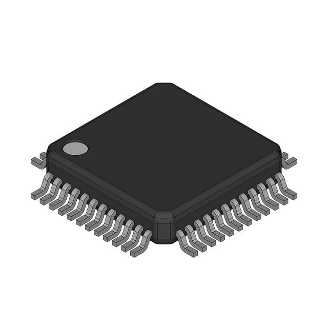
- Part No.:
- AD8381JST
- Manufacturer:
- Analog Devices Inc.
- Category:
- Display Drivers
- Package:
- 48-LQFP
- Datasheet:
-
 AD8381JST.pdf
- Description:
- LIQUID CRYSTAL DRIVER, 6-SEGMENT
- Quantity:
- Payment:

- Shipping:

Inventory:2,157
Please send an inquiry. Send us your inquiry, and we will respond immediately.
Product details
Overview
AD8381 from Analog Devices is a fast, high-voltage 6-channel LCD column driver IC with 10-bit resolution, 100 Ms/s input data rate, ±1.3 V rail-to-rail output swing (at AVCC = 15.5 V), and 27 ns settling time to 1% into 150 pF - designed for driving analog column electrodes in high-resolution projection LCD panels.
For engineers reviewing the AD8381 datasheet, AD8381 pinout, AD8381 application, or AD8381 equivalent, key selection considerations include its decimating latch architecture, dual-mode polarity control (INV), even/odd synchronization (E/O + STSQ), flexible reference scaling (VREFHI/VREFLO/VMID), and integrated overload protection for robust panel driving under capacitive load.
Technical Context
The AD8381 integrates six independent 10-bit bipolar DACs with precision current-feedback output amplifiers on a proprietary 24 V fast bipolar process, enabling sub-32 ns data-switching settling and 410 V/µs invert-switching slew rate. Its two-stage latch architecture supports sequential loading of six 10-bit words per cycle via DB(0:9) with programmable direction (R/L) and edge-triggered timing (E/O).
It implements voltage-controlled full-scale (VFS = 2 × (VREFHI – VREFLO)) and midpoint (VMID) references, allowing real-time brightness/contrast adjustment and polarity inversion (INV) without external components. Standby mode (STBY) reduces total quiescent current to ≤3 mA while preserving system-level timing coordination across multi-chip configurations.
Key Specifications
| Parameter | Value and Actual Design Meaning |
|---|---|
| Resolution | 10-bit binary input - supports 1024 grayscale levels per channel with laser-trimmed DAC matching. |
| Data Rate | 100 Ms/s NRZ - enables real-time pixel streaming for XGA/SXGA projectors at ≥75 Hz refresh. |
| Output Swing | Within 1.3 V of AVCC/AGND rails - delivers full dynamic range into high-voltage LCD bias schemes. |
| Settling Time | 27 ns to 1% into 150 pF - ensures minimal ghosting during rapid video transitions. |
| Power Dissipation | 570 mW nominal - optimized for thermal management in compact projector engine PCB layouts. |
| Reference Flexibility | VREFHI/VREFLO sets VFS (0–5.75 V); VMID sets common-mode level (6.25–9.25 V) - enables precise gamma and offset tuning. |
| Protection | Internal 100 mA average current limit + thermal shutdown - prevents damage during panel short events. |
Pinout & Package
AD8381 is housed in a 48-lead LQFP (7 mm × 7 mm × 1.4 mm, ST-48 package) with exposed pad for thermal performance. Digital and analog sections are physically segregated on opposite sides to minimize crosstalk.
| Pin/Terminal | Circuit Role | Design Meaning |
|---|---|---|
| DB(0:9) | 10-bit parallel data bus | MSB-aligned input for sequential 6-word loading; supports NRZ at 100 Ms/s with zero setup time. |
| VID0–VID5 | Analog video outputs | Direct-drive outputs for LCD column electrodes; each capable of ±75 mA sink/source into 150 pF. |
| CLK, STSQ, XFR | Timing control inputs | Edge-triggered sequence initiation (STSQ), synchronous output update (XFR), and clock (CLK) with 5 ns rise/fall tolerance. |
| INV, R/L, E/O | Digital configuration inputs | Real-time polarity inversion (INV), left/right loading direction (R/L), and even/odd edge selection (E/O) for multi-chip synchronization. |
| VREFHI/VREFLO/VMID | Analog reference inputs | Externally set full-scale (VFS) and midpoint (VMID) voltages - define transfer function slope and offset independently. |
| AVCCx, AGNDx, DVCC, DGND | Power supply terminals | Separate 9–18 V analog (AVCC) and 3–5.5 V digital (DVCC) rails with dedicated ground returns per section. |
| STBY, BYP | Power management | Standby mode reduces AVCC/DVCC current to ≤3 mA/0.1 mA; BYP requires 0.1 µF to AGND for optimal settling. |
Key Features
| Feature | Design Value |
|---|---|
| Decimating latch architecture | Loads six 10-bit words sequentially per STSQ cycle - eliminates need for external FIFO or frame buffer in projector timing engines. |
| Voltage-controlled reference scaling | VREFHI/VREFLO sets full-scale (0–5.75 V); VMID sets common-mode (6.25–9.25 V) - enables dynamic contrast/brightness adjustment without recalibration. |
| Programmable polarity & direction | INV pin toggles transfer function slope (positive/negative); R/L selects loading order (Ch0→Ch5 or Ch5→Ch0) - supports image mirroring and column inversion. |
| Multi-chip synchronization | E/O and STSQ enable deterministic interleaving of two AD8381s for 12-channel systems - maintains pixel alignment without external glue logic. |
| Integrated overload protection | Two-stage protection (current limit + thermal shutdown) sustains infinite short-circuit duration at outputs - enhances field reliability in panel manufacturing environments. |
Applications
| LCD Projection Engine | High-Resolution Data Projector |
|---|---|
Use Scenario: Driving analog column electrodes in SXGA+ (1400×1050) transmissive LCD panels within compact DLP-style optical engines. IC Role / Device Role / Timing Role: Primary column driver IC; receives pixel data from image processor via 10-bit parallel bus and updates all six channels synchronously on XFR edge. Use Value: 27 ns settling time and 100 Ms/s data rate eliminate motion blur at 75 Hz refresh; rail-to-rail swing maximizes panel contrast ratio. |
Use Scenario: Dual-AD8381 configuration in UXGA (1600×1200) projector supporting 75 Hz progressive scan with column inversion. IC Role / Device Role / Timing Role: One AD8381 operates in Even mode (E/O = H), the other in Odd mode (E/O = L); both share CLK and DB(0:9) with staggered STSQ timing. Use Value: Eliminates need for dual-data-bus FPGA interface; E/O + STSQ coordination ensures pixel-perfect interleave without skew. |
| Industrial LCD Display Controller | Medical Imaging Monitor Driver |
Use Scenario: Driving custom high-brightness LCD modules in factory automation HMIs requiring stable grayscale linearity over 0–85°C. IC Role / Device Role / Timing Role: Column driver with laser-trimmed DACs and VMID/VREFHI/VREFLO calibration points - referenced to external precision voltage sources. Use Value: <±7.5 mV differential error (VDE) and <±3.5 mV common-mode error (VCME) ensure consistent grayscale rendering across temperature. |
Use Scenario: Driving diagnostic-grade monochrome LCD panels in ultrasound or MRI console displays where grayscale fidelity is critical. IC Role / Device Role / Timing Role: High-accuracy 10-bit DAC with INV-controlled polarity switching - enables real-time pixel inversion to reduce image retention. Use Value: Invert-switching slew rate of 410 V/µs and <100 ns thermal recovery support rapid polarity reversal without visible artifacts. |
Equivalent & Alternatives
The following parts are listed as comparable options for similar LCD column driver applications.
| Alternative Part | Technical Difference | Application Difference | Selection Advice |
|---|---|---|---|
| TLC5940IPWP | 16-channel, 12-bit PWM LED driver; no analog output, no high-voltage capability (max 17 V), no VMID/VREFHI scaling. | Designed for LED current sinking, not LCD voltage column driving; lacks rail-to-rail analog swing and video timing controls (STSQ/XFR/INV). | Select only if driving LED backlights - not suitable as functional replacement for AD8381's analog LCD column role. |
| THS8135IPHP | Triple 10-bit video DAC with 300 MSPS; single-ended outputs, max ±3.5 V swing, no integrated overload protection, no STSQ/XFR protocol. | Targets RGB video signal reconstruction (e.g., VGA DAC), not multiplexed column addressing; lacks sequencer logic and panel-specific protection. | Use for general-purpose video DAC applications; not viable for direct LCD column driving due to voltage range and missing control architecture. |
Compared with TLC5940IPWP and THS8135IPHP, the AD8381 uniquely combines 6-channel analog column drive, programmable polarity inversion, synchronized multi-chip operation, and integrated protection - making it irreplaceable in high-reliability LCD projection systems where timing determinism and voltage margin are critical.
Availability
AD8381 is available at Aetrix Electronics and suitable for LCD projection engines, high-resolution data projectors, industrial display controllers, and medical imaging monitor drivers requiring stable component supply and long-term BOM continuity.
Supply support for AD8381 includes scheduled delivery planning, volume procurement assistance, BOM continuity management, traceable sourcing, and lifecycle availability coordination for OEM customers, industrial embedded developers, connected-device designers, and electronics production programs.
Manufacturer
Analog Devices, Inc. is a global leader in high-performance analog, mixed-signal, and digital signal processing semiconductors, headquartered in Norwood, MA.
The AD8381 belongs to Analog Devices' DecDriver® family of high-speed LCD panel drivers, engineered specifically for demanding projection and industrial display applications requiring precision analog output, fast settling, and robust multi-chip synchronization.
FAQ
What is the maximum full-scale output voltage supported by the AD8381?
The AD8381 supports a maximum full-scale output voltage (VFS) of 5.75 V, defined as VFS = 2 × (VREFHI – VREFLO). This limit is enforced by the internal scale factor control loop and remains valid across the operating temperature range (0°C to 85°C) when VMID is within its specified 6.25 V to 9.25 V range. Exceeding this value degrades linearity and may trigger output clipping.
How does the INV pin affect the AD8381 transfer function?
The INV pin selects between two complementary transfer functions: when low, VOUT increases from (VMID – VFS) to VMID as input code rises from 0 to 1023; when high, VOUT decreases from (VMID + VFS) to VMID. This enables real-time polarity inversion for column/row/pixel inversion schemes without external circuitry - a core feature used in the AD8381 for flicker reduction in LCD panels.
Can multiple AD8381 devices be synchronized for 12-channel operation?
Yes - two AD8381 devices can be synchronized for 12-channel operation using the E/O, STSQ, and XFR pins. One device is configured for even-numbered channels (E/O = HIGH), the other for odd (E/O = LOW); both share the same DB(0:9) bus and CLK, with STSQ edges staggered to initiate alternating 6-word sequences. This eliminates external sequencing logic and ensures deterministic pixel alignment.
What is the purpose of the VMID pin on the AD8381?
The VMID pin sets the midpoint reference voltage for all six analog outputs. It defines the center of the transfer function - e.g., when INV = LOW, output ranges from (VMID – VFS) to VMID; when INV = HIGH, from VMID to (VMID + VFS). VMID must be externally supplied between 6.25 V and 9.25 V and is typically connected to the LCD panel's VCOM node to maintain common-mode stability.
Does the AD8381 include built-in protection against output short circuits?
Yes - the AD8381 incorporates a two-stage overload protection circuit: an internal current limiter restricts output current to ≤100 mA average per channel, and a thermal shutdown circuit disables the output amplifier if junction temperature exceeds ~150°C. Recovery from momentary shorts is ~100 ns; thermal recovery depends on ambient conditions but ensures long-term reliability during sustained fault conditions.
AD8381JST Specifications
- Product attributes
- Attribute value
- Manufacturer:
- Analog Devices Inc.
- Series:
- AD8381
- Package/Case:
- 48-LQFP
- Packaging:
- Bulk
- Product Status:
- Active
- Display Type:
- LCD
- Configuration:
- -
- Interface:
- -
- Digits or Characters:
- -
- Current - Supply:
- 33 mA
- Voltage - Supply:
- 3V ~ 5.5V, 9V ~ 18V
- Operating Temperature:
- 0°C ~ 85°C
- Grade:
- -
- Qualification:
- -
- Mounting Type:
- Surface Mount
- Supplier Device Package:
- 48-LQFP (7x7)
AD8381JST FAQ
1.How can I place an order for AD8381JST through Aetrix?
Please submit a Request for Quotation (RFQ) for AD8381JST on Aetrix. Our sales agent will provide a competitive quotation and guide you through the order confirmation once you accept the terms.
2.Are the price and stock information for AD8381JST reliable?
The price and inventory of AD8381JST are updated periodically and may fluctuate due to market conditions. Stock and pricing data are typically refreshed every 24 hours. Quotation validity for AD8381JST is usually 5 days.
3.What payment methods are accepted for AD8381JST?
We accept Wire Transfer, PayPal, Credit Card, Western Union, MoneyGram, and Escrow for AD8381JST transactions.
Note: Certain payment methods may incur a processing fee.
4.How is shipping managed for AD8381JST?
AD8381JST orders can be shipped via leading logistics carriers, including DHL, UPS, FedEx, TNT, or Registered Mail.
Once your AD8381JST order is processed, you will receive an email with the shipment details and tracking number.
Note: Tracking information may take up to 24 hours to appear. Express delivery typically takes 3–5 business days.
5.How can I obtain technical support or documentation for AD8381JST?
For technical support, including AD8381JST datasheets, pinout diagrams, or application guidance, please contact our engineering support team. They can provide detailed documentation and assistance for your AD8381JST requirements.
6.How does Aetrix verify that AD8381JST is sourced from the original manufacturer or authorized distributors?
All AD8381JST products on Aetrix are procured from qualified distributors and authorized channels. Our dedicated quality assurance team conducts strict verification, including traceability checks and, if necessary, third-party testing. This ensures that AD8381JST meets industry standards.
7.What is the process for return or replacement of AD8381JST?
All AD8381JST units undergo pre-shipment inspection (PSI). If there is an issue with AD8381JST, returns or replacements are accepted under the following conditions:
1.Quantity discrepancies, incorrect items, or visible external defects (such as breakage or corrosion), acknowledged by Aetrix.
2.The issue is reported within 90 days of delivery.
3.The AD8381JST part is unused and in its original packaging.
Return procedure for AD8381JST:
1.Submit a request within 90 days.
2.Obtain a Return Material Authorization (RMA) from Aetrix.
AD8381JST Tags
-
PCA8561AHN/AY
NXP Semiconductors

-
SN74LS47N
Texas Instruments

-
PCF85176T/1Y
NXP Semiconductors
-
PCF85176H/1,518
NXP Semiconductors
-
BU9796AMUV-E2
Rohm Semiconductor
-
PCA85176H/Q900/1,5
NXP Semiconductors
-
PCF8537AH/1,518
NXP Semiconductors
-
LM3914VX/NOPB
Texas Instruments

-
PCF85134HL/1,118
NXP Semiconductors
-
AS1115-BSST
ams-OSRAM USA INC.
-
PCA8534AH/Q900/1,5
NXP Semiconductors
-
LM3914V/NOPB
Texas Instruments
Tech Hub

A practical engineering guide to 3.3V and 5V logic compatibility, input thresholds, resistor dividers, translator ICs, MOSFET level shifting, I2C pull-ups, timing limits and power-sequencing risks.

The 74HC595 uses push-pull logic outputs, while the TPIC6B595 uses 50 V open-drain DMOS sinks for higher-power loads. This guide compares timing, current limits, 3.3 V interfacing, load wiring, thermal…

The 74HC595 converts serial data into eight stable parallel outputs. This guide covers pin functions, shift and storage timing, OE and MR behavior, drive-current limits, cascading, voltage compatibilit…

A technical comparison of level-sensitive latches and edge-triggered flip-flops, covering timing windows, setup and hold limits, master–slave operation, time borrowing, race-through, HDL inference and…

A D latch stores one bit while Enable controls when data can pass. This reference covers gate-level operation, truth tables, transparency, setup and hold timing, LE versus OE, common ICs and practical …

An SR latch stores one bit through cross-coupled feedback. This engineering reference covers NOR and NAND implementations, truth tables, forbidden-state recovery, gated operation, switch debouncing, fa…

Latch circuits retain one bit through feedback. This technical reference covers SR and D latches, truth tables, transparency, timing limits, latch-versus-flip-flop behavior, applications and common log…

An engineering guide to LED driver operation, constant-current and constant-voltage outputs, linear and switching topologies, dimming, IC selection, calculations, replacement compatibility, and fault c…

Operational amplifier guide covering op amp basics, feedback, ideal vs real op amps, common configurations, buffer circuits, offset, bias current, gain-bandwidth, slew rate, rail-to-rail limits and sel…

Jumper cables guide covering safe connection order, red and black clamp placement, final ground connection, cable gauge, length, clamp quality, copper vs CCA cables, jump starter comparison and battery…


