
 My Inquiry
 My Account


Analog Devices Inc. AD9397KSTZ-150
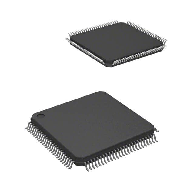
- Part No.:
- AD9397KSTZ-150
- Manufacturer:
- Analog Devices Inc.
- Category:
- Specialized
- Package:
- 100-LQFP
- Datasheet:
-
 AD9397KSTZ-150.pdf
- Description:
- IC INTERFACE 150MHZ DVI 100LQFP
- Quantity:
- Payment:

- Shipping:

Inventory:4,255
Please send an inquiry. Send us your inquiry, and we will respond immediately.
Product details
Overview
AD9397KSTZ-150 from Analog Devices is a DVI 1.0-compliant digital video receiver IC with integrated HDCP 1.1 decryption, supporting up to 150 MHz pixel clock, 1080p/720p HDTV formats, and RGB ↔ YCbCr color space conversion. It operates with dual supply rails (3.3 V VD / 1.8 V DVDD), delivers 24-bit parallel RGB/YCbCr outputs, and targets front-end video interface applications in flat-panel displays and projectors.
For engineers reviewing the AD9397KSTZ-150 datasheet, AD9397KSTZ-150 pinout, AD9397KSTZ-150 application, or AD9397KSTZ-150 equivalent, key selection considerations include TMDS input skew tolerance (1 full clock cycle), programmable DATACK phase alignment, HDCP key storage architecture, and 100-lead LQFP package compatibility with high-density video PCB layouts.
Technical Context
The AD9397KSTZ-150 implements a fully integrated DVI 1.0 receiver with three TMDS data channel pairs (Rx0±, Rx1±, Rx2±) and one TMDS clock pair (RxC±), all internally terminated to 50 Ω via RTERM-controlled 500 Ω resistor. Its HDCP 1.1 engine authenticates receivers, decrypts encrypted streams, and supports key renewability during active transmission using external EEPROM interfacing via MDA/MCL and DDCSDA/DDCSCL I²C buses.
It features a programmable color space converter (CSC) supporting RGB ↔ YCbCr bidirectional conversion at up to 150 MHz, configurable output formats (RGB 24-bit, YCbCr 4:4:4 or 4:2:2), and pixel sampling phase adjustment across 32 steps (0–360°) for optimal eye diagram alignment. Output timing maintains fixed relationships among DATACK, HSOUT, VSOUT, and DE through synchronous PLL-derived clocks.
Key Specifications
| Parameter | Value and Actual Design Meaning |
|---|---|
| Max Pixel Clock | 150 MHz - supports SXGA (1280×1024@80 Hz), 1080p60, and 720p60 display resolutions without undersampling. |
| HDCP Version | HDCP 1.1 - enables secure authentication and decryption of encrypted DVI video streams per HDMI/DVI compliance requirements. |
| Input Interface | 3× TMDS data + 1× TMDS clock - differential inputs compliant with DVI 1.0 electrical specs; intrapair skew tolerance ≤1 clock cycle. |
| Output Format | RGB 8×3 or YCbCr 4:2:2/4:4:4 - parallel 24-bit digital outputs with selectable color space, bit depth (8/10/12-bit), and timing alignment. |
| Supply Voltages | VD = 3.3 V (analog/TMDS), DVDD = PVDD = 1.8 V (digital/PLL), VDD = 1.8–3.3 V (output logic) - enables mixed-voltage system interfacing. |
| Package | 100-lead Pb-free LQFP - surface-mount footprint with exposed thermal pad; specified for 0°C to 70°C industrial temperature range. |
| Power Dissipation | 1.4 W typical - includes active-mode power for full-rate 150 MHz operation; drops to 130 mW in power-down mode. |
Pinout & Package
AD9397KSTZ-150 is housed in a 100-lead, Pb-free, thermally enhanced LQFP package (14 mm × 14 mm, 0.5 mm pitch) with exposed thermal pad. Pin 1 marked by dot; pins arranged in four sides with GND, power, and signal groups distributed to minimize noise coupling.
| Pin/Terminal | Circuit Role | Design Meaning |
|---|---|---|
| Rx0+/Rx0− | TMDS Channel 0 Differential Input | Receives red-component pixel data; requires 100 Ω differential PCB trace impedance and internal 50 Ω termination to VD. |
| Rx1+/Rx1− | TMDS Channel 1 Differential Input | Receives green-component pixel data; matched routing critical to maintain <360 ps intrapair skew and <6 ps channel-to-channel skew. |
| Rx2+/Rx2− | TMDS Channel 2 Differential Input | Receives blue-component pixel data; shares same termination and layout rules as Rx0/Rx1 channels. |
| RxC+/RxC− | TMDS Clock Differential Input | Carries 1× pixel rate clock; used for sampling all three data channels; phase-aligned to data for setup/hold margin optimization. |
| RED[7:0]/GREEN[7:0]/BLUE[7:0] | Parallel Digital Video Outputs | 24-bit RGB output bus; MSB-aligned, VDD-referenced (1.8–3.3 V); timing locked to DATACK rising edge for reliable latching. |
| DATACK | Data Output Clock | Programmable pixel-synchronous clock (1×, 2×, ½×, or 90°-shifted); strobes output data and sync signals into downstream logic. |
| HSOUT/VSOUT/DE/FIELD | Reconstructed Timing Signals | Phase-aligned HSYNC/VSYNC, data enable, and interlaced odd/even field indicators - all derived from TMDS stream and adjustable via registers. |
| SCL/SDA | Main Serial Control Port | I²C interface (7-bit address 0x98) for configuration register access, CSC matrix loading, and power mode control. |
| DDCSCL/DDCSDA | HDCP Slave Port | I²C interface (addresses 0x74/0x76) for real-time HDCP authentication handshake with DVI transmitter. |
| MCL/MDA | HDCP Master Port | I²C interface (address 0xA0) for reading HDCP keys from external EEPROM; essential for HDCP 1.1 compliance. |
Key Features
| Feature | Design Value |
|---|---|
| Integrated HDCP 1.1 Engine | Enables secure playback of protected content without external crypto IC; supports key renewability and authentication retries during active link. |
| Programmable Color Space Converter | Full RGB ↔ YCbCr conversion at 150 MHz with 13-bit coefficient resolution; supports 4:2:2 downconversion with minimal chroma aliasing. |
| Pixel Sampling Phase Adjustment | 32-step (0–360°) fine-tuning of sampling point relative to HSYNC - maximizes data eye opening for marginal TMDS links. |
| Reconstructed Sync Outputs | HSOUT, VSOUT, DE, and FIELD outputs maintain deterministic timing relationships to DATACK - eliminates need for external sync re-timing logic. |
| Multi-Rail Power Architecture | Separate VD (3.3 V analog), DVDD/PVDD (1.8 V digital/PLL), and VDD (1.8–3.3 V I/O) supplies isolate noise-sensitive circuitry and support mixed-voltage systems. |
Applications
| Advanced TV Receivers | HDTV Display Front-End |
|---|---|
|
Use Scenario: Receiving HDCP-encrypted DVI video from set-top boxes or Blu-ray players in premium television sets. IC Role / Device Role / Timing Role: DVI receiver and HDCP authenticator; reconstructs clean RGB/YCbCr outputs and timing signals for internal scaler or panel driver. Use Value: Eliminates need for discrete HDCP controller and TMDS receiver; reduces BOM count and PCB area while ensuring content protection compliance. |
Use Scenario: Converting incoming DVI signals to YCbCr 4:2:2 format for processing by video scalers or frame buffers in HDTV monitors. IC Role / Device Role / Timing Role: Color space converter and timing generator; provides phase-aligned DATACK, HSOUT, and VSOUT synchronized to pixel clock. Use Value: Offloads color conversion from main processor; preserves signal fidelity with hardware-accelerated 4:4:4 → 4:2:2 filtering and precise pixel sampling control. |
| Professional Projectors | LCD Monitor Video Interface |
|
Use Scenario: Accepting high-resolution DVI sources (e.g., medical imaging, CAD workstations) in fixed-installation projectors requiring stable, low-jitter video capture. IC Role / Device Role / Timing Role: High-bandwidth DVI receiver with intrapair skew correction; generates jitter-free DATACK and reconstructed syncs for FPGA-based image processing pipelines. Use Value: Enables reliable 1080p60 capture with <±2 ns clock-to-data skew - critical for zero-frame-drop rendering in mission-critical visualization systems. |
Use Scenario: Interfacing desktop PCs and gaming consoles to LCD panels via DVI-D cables in commercial monitors. IC Role / Device Role / Timing Role: DVI receiver with DE generation and RGB output formatting; handles variable refresh rates and EDID communication via DDC ports. Use Value: Supports plug-and-play compatibility with legacy and modern graphics cards; simplifies EDID management and HDCP negotiation without firmware overhead. |
Equivalent & Alternatives
The following parts are listed as comparable options for similar DVI receiver applications.
| Alternative Part | Technical Difference | Application Difference | Selection Advice |
|---|---|---|---|
| TI TFP401APZPR | No integrated HDCP; requires external HDCP controller; supports up to 165 MHz pixel clock; 100-pin TQFP. | Targeted at non-HDCP systems or where external HDCP key management is preferred; lacks on-chip CSC and DE generation. | Select when HDCP is not required and higher bandwidth (>150 MHz) is needed; verify external HDCP implementation complexity. |
| Maxim MAX9516ETL+ | Lower bandwidth (135 MHz); no HDCP; integrated video amplifier and sync separator; 28-pin TQFN. | Designed for analog CVBS/S-video to digital RGB conversion, not native DVI reception; no TMDS input capability. | Not a functional substitute - only relevant for hybrid analog/digital video front-ends lacking DVI/HDCP requirements. |
Compared with TFP401APZPR and MAX9516ETL+, the AD9397KSTZ-150 uniquely integrates HDCP 1.1, programmable CSC, and full DVI 1.0 receiver functionality in a single 100-lead LQFP, reducing system-level design effort for secure, high-fidelity digital display interfaces.
Availability
AD9397KSTZ-150 is available at Aetrix Electronics and suitable for advanced TV receivers, HDTV display front-ends, and professional projector designs requiring stable component supply, long-term lifecycle support, and guaranteed authenticity of Analog Devices silicon.
Supply support for AD9397KSTZ-150 includes scheduled delivery planning, volume procurement assistance, BOM continuity management, traceable sourcing, and lifecycle availability coordination for OEM customers, industrial embedded developers, connected-device designers, and electronics production programs.
Manufacturer
Analog Devices, Inc. is a global leader in high-performance analog, mixed-signal, and digital signal processing semiconductors, headquartered in Norwood, MA.
The AD9397KSTZ-150 belongs to Analog Devices' high-speed video interface product line, designed specifically for secure, low-latency DVI reception in premium consumer and professional display equipment.
FAQ
What is the maximum supported pixel clock frequency for the AD9397KSTZ-150?
The AD9397KSTZ-150 supports a maximum pixel clock frequency of 150 MHz, enabling full support for 1080p60, 720p60, and SXGA (1280×1024@80 Hz) display resolutions. This rating is confirmed in Table 1 and Table 2 of the Rev. 0 datasheet under AC specifications for AD9397KSTZ-150, with DATACK frequency (FCIP) specified as 20–150 MHz.
Does the AD9397KSTZ-150 include built-in HDCP functionality?
Yes, the AD9397KSTZ-150 integrates a complete HDCP 1.1 engine with internal key storage architecture. It performs receiver authentication, encrypted data decryption, and key renewability during active transmission, as documented in the General Description and HDCP section of the datasheet. External EEPROM interfacing via MCL/MDA is required for key provisioning.
Can the AD9397KSTZ-150 convert RGB input to YCbCr output?
Yes, the AD9397KSTZ-150 features a fully programmable color space converter (CSC) that supports bidirectional RGB ↔ YCbCr conversion. It accepts RGB input and outputs YCbCr in 4:4:4 or 4:2:2 formats at up to 150 MHz, with 13-bit coefficient resolution and dedicated filter for 4:4:4 → 4:2:2 downconversion, as detailed in the Color Space Conversion section.
What package type and lead count does the AD9397KSTZ-150 use?
The AD9397KSTZ-150 uses a 100-lead, Pb-free LQFP package (14 mm × 14 mm, 0.5 mm pitch) with exposed thermal pad. This is explicitly stated in the Features list and confirmed in the Outline Dimensions section (Page 28) and Pin Configuration diagram (Figure 2) of the Rev. 0 datasheet.
How is power managed on the AD9397KSTZ-150?
The AD9397KSTZ-150 implements four power states - full-power, seek mode, auto power-down, and power-down - controlled via serial register 0x26 and PWRDN pin. Power-down dissipation is 130 mW, and supply sequencing must ensure VD and VDD remain within ±300 mV of DVDD, as defined in the Power Management and Power Supply sections (Pages 10–11).
AD9397KSTZ-150 Specifications
- Product attributes
- Attribute value
- Manufacturer:
- Analog Devices Inc.
- Series:
- -
- Package/Case:
- 100-LQFP
- Packaging:
- Tray
- Product Status:
- Obsolete
- Applications:
- Video
- Interface:
- DVI
- Voltage - Supply:
- 3.15V ~ 3.47V
- Supplier Device Package:
- 100-LQFP (14x14)
- Grade:
- -
- Qualification:
- -
- Mounting Type:
- Surface Mount
AD9397KSTZ-150 FAQ
1.How can I place an order for AD9397KSTZ-150 through Aetrix?
Please submit a Request for Quotation (RFQ) for AD9397KSTZ-150 on Aetrix. Our sales agent will provide a competitive quotation and guide you through the order confirmation once you accept the terms.
2.Are the price and stock information for AD9397KSTZ-150 reliable?
The price and inventory of AD9397KSTZ-150 are updated periodically and may fluctuate due to market conditions. Stock and pricing data are typically refreshed every 24 hours. Quotation validity for AD9397KSTZ-150 is usually 5 days.
3.What payment methods are accepted for AD9397KSTZ-150?
We accept Wire Transfer, PayPal, Credit Card, Western Union, MoneyGram, and Escrow for AD9397KSTZ-150 transactions.
Note: Certain payment methods may incur a processing fee.
4.How is shipping managed for AD9397KSTZ-150?
AD9397KSTZ-150 orders can be shipped via leading logistics carriers, including DHL, UPS, FedEx, TNT, or Registered Mail.
Once your AD9397KSTZ-150 order is processed, you will receive an email with the shipment details and tracking number.
Note: Tracking information may take up to 24 hours to appear. Express delivery typically takes 3–5 business days.
5.How can I obtain technical support or documentation for AD9397KSTZ-150?
For technical support, including AD9397KSTZ-150 datasheets, pinout diagrams, or application guidance, please contact our engineering support team. They can provide detailed documentation and assistance for your AD9397KSTZ-150 requirements.
6.How does Aetrix verify that AD9397KSTZ-150 is sourced from the original manufacturer or authorized distributors?
All AD9397KSTZ-150 products on Aetrix are procured from qualified distributors and authorized channels. Our dedicated quality assurance team conducts strict verification, including traceability checks and, if necessary, third-party testing. This ensures that AD9397KSTZ-150 meets industry standards.
7.What is the process for return or replacement of AD9397KSTZ-150?
All AD9397KSTZ-150 units undergo pre-shipment inspection (PSI). If there is an issue with AD9397KSTZ-150, returns or replacements are accepted under the following conditions:
1.Quantity discrepancies, incorrect items, or visible external defects (such as breakage or corrosion), acknowledged by Aetrix.
2.The issue is reported within 90 days of delivery.
3.The AD9397KSTZ-150 part is unused and in its original packaging.
Return procedure for AD9397KSTZ-150:
1.Submit a request within 90 days.
2.Obtain a Return Material Authorization (RMA) from Aetrix.
AD9397KSTZ-150 Tags

-
NVT4857UKAZ
NXP Semiconductors

-
TCA8418RTWR
Texas Instruments

-
PCA9546APWR
Texas Instruments

-
MD0100N8-G
Microchip Technology

-
PCA9548APW,118
NXP Semiconductors

-
PCA9540BDP,118
NXP Semiconductors

-
PCA9548APWR
Texas Instruments

-
PCA9546APW,118
NXP Semiconductors

-
PTN3360DBS,518
NXP Semiconductors

-
PCA9546ABS,118
NXP Semiconductors

-
PCA9518PWR
Texas Instruments

-
PCA9545APW,118
NXP Semiconductors
Tech Hub

A practical engineering guide to 3.3V and 5V logic compatibility, input thresholds, resistor dividers, translator ICs, MOSFET level shifting, I2C pull-ups, timing limits and power-sequencing risks.

The 74HC595 uses push-pull logic outputs, while the TPIC6B595 uses 50 V open-drain DMOS sinks for higher-power loads. This guide compares timing, current limits, 3.3 V interfacing, load wiring, thermal…

The 74HC595 converts serial data into eight stable parallel outputs. This guide covers pin functions, shift and storage timing, OE and MR behavior, drive-current limits, cascading, voltage compatibilit…

A technical comparison of level-sensitive latches and edge-triggered flip-flops, covering timing windows, setup and hold limits, master–slave operation, time borrowing, race-through, HDL inference and…

A D latch stores one bit while Enable controls when data can pass. This reference covers gate-level operation, truth tables, transparency, setup and hold timing, LE versus OE, common ICs and practical …

An SR latch stores one bit through cross-coupled feedback. This engineering reference covers NOR and NAND implementations, truth tables, forbidden-state recovery, gated operation, switch debouncing, fa…

Latch circuits retain one bit through feedback. This technical reference covers SR and D latches, truth tables, transparency, timing limits, latch-versus-flip-flop behavior, applications and common log…

An engineering guide to LED driver operation, constant-current and constant-voltage outputs, linear and switching topologies, dimming, IC selection, calculations, replacement compatibility, and fault c…

Operational amplifier guide covering op amp basics, feedback, ideal vs real op amps, common configurations, buffer circuits, offset, bias current, gain-bandwidth, slew rate, rail-to-rail limits and sel…

Jumper cables guide covering safe connection order, red and black clamp placement, final ground connection, cable gauge, length, clamp quality, copper vs CCA cables, jump starter comparison and battery…


