
 My Inquiry
 My Account


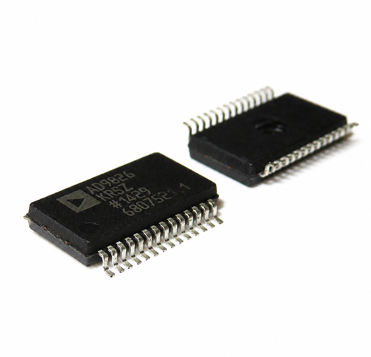
Analog Devices Inc. AD9826KRSZ
- Part No.:
- AD9826KRSZ
- Manufacturer:
- Analog Devices Inc.
- Category:
- Sensor and Detector Interfaces
- Package:
- 28-SSOP (0.209", 5.30mm Width)
- Datasheet:
-
 AD9826KRSZ.pdf
- Description:
- IC IMAGE SGNL PROC 16BIT 28-SSOP
- Quantity:
- Payment:

- Shipping:

Inventory:5,200
Please send an inquiry. Send us your inquiry, and we will respond immediately.
Product details
Overview
AD9826KRSZ from Analog Devices Inc. is a complete 16-bit imaging signal processor designed to sample, condition, and digitize CCD, CIS, CMOS active pixel sensor, and focal-plane-array signals. The device integrates three analog input channels, input clamp circuitry, correlated double sampling, programmable offset DACs, programmable gain amplifiers, a 3:1 multiplexer, a 16-bit ADC, internal voltage reference, 8-bit multiplexed digital output, and a 3-wire serial control interface.
For engineers reviewing the AD9826KRSZ datasheet, AD9826KRSZ pinout, AD9826KRSZ application, or AD9826KRSZ equivalent, this part is most relevant for flatbed document scanners, digital copiers, multifunction peripherals, infrared imaging systems, and machine-vision signal chains requiring 16-bit image acquisition, RGB channel processing, 1× to 6× programmable gain, ±300 mV offset adjustment, and 28-lead SSOP assembly.
Technical Context
AD9826KRSZ uses a 3-channel architecture for trilinear color CCD arrays, with VINR, VING, and VINB processed through clamp, CDS, offset DAC, and PGA stages before conversion by the shared 16-bit ADC. It supports 3-channel 16-bit operation up to 15 MSPS, 1-channel 16-bit operation up to 12.5 MSPS, and a 2-channel mode for mono sensors with odd/even outputs.
The analog signal chain provides 2.0 V p-p or 4.0 V p-p programmable input range, 1× to 6× PGA gain in 64 steps, ±300 mV programmable offset in 512 steps, and 70 dB channel-to-channel crosstalk at 15 MSPS. AVDD operates from 4.75 V to 5.25 V, while DRVDD supports 3.0 V to 5.25 V digital output operation for 3 V or 5 V logic interfaces.
Key Specifications
| Parameter | Value and Actual Design Meaning |
|---|---|
| Device Type | Complete 16-bit imaging signal processor for CCD, CIS, CMOS sensor, and focal-plane-array front ends. |
| ADC Resolution | 16-bit ADC with no missing codes guaranteed, supporting high-resolution image signal conversion. |
| Channel Architecture | Three analog channels for Red, Green, and Blue inputs, multiplexed into one high-performance ADC. |
| Operating Modes | 3-channel CDS, 3-channel SHA, 2-channel CDS, 2-channel SHA, 1-channel CDS, and 1-channel SHA modes selected through internal registers. |
| Conversion / Pixel Operation | 3-channel 16-bit operation up to 15 MSPS and 1-channel 16-bit operation up to 12.5 MSPS for imaging acquisition timing. |
| Input Signal Range | Programmable 2.0 V p-p or 4.0 V p-p input range, allowing adaptation to different sensor output amplitudes. |
| PGA Gain | 1× to 6× programmable gain in 64 steps for Red, Green, and Blue channel scaling. |
| Programmable Offset | ±300 mV offset adjustment in 512 steps for per-channel black-level and signal-offset correction. |
| Digital Interface | 3-wire serial interface using SDATA, SCLK, and SLOAD for register programming. |
| Digital Output | 8-bit D7 to D0 multiplexed output carrying 16-bit ADC data over two read cycles, with optional single-byte output mode. |
| Supply Voltage | AVDD 4.75 V to 5.25 V; DRVDD 3.0 V to 5.25 V for 3 V / 5 V digital I/O compatibility. |
| Power Dissipation | 400 mW typical in 3-channel mode and 300 mW typical in 1-channel mode, with 200 μA power-down current. |
| Operating Temperature | -40 °C to +85 °C for the AD9826KRSZ ordering option. |
| Package | 28-lead Shrink Small Outline Package [SSOP], package option RS-28, RoHS compliant Z suffix. |
Pinout & Package
AD9826KRSZ is supplied in a 28-lead Shrink Small Outline Package [SSOP], package option RS-28, compliant with JEDEC MO-150-AH. The SSOP package uses a 0.65 mm lead pitch with a compact body format, helping imaging front-end boards route analog sensor inputs, ADC clocks, serial-control pins, and byte-wide digital outputs in space-constrained scanner, copier, and machine-vision layouts.
| Pin / Terminal | Circuit Role | Design Meaning |
|---|---|---|
| VINR, VING, VINB | Red, Green, and Blue analog input channels. | Receive image-sensor output signals for 3-channel acquisition; each channel feeds the clamp, CDS or SHA path, offset DAC, and PGA before multiplexing to the ADC. |
| CDSCLK1, CDSCLK2 | Correlated double sampling timing inputs. | Control reference-level and data-level sampling in CDS mode, allowing the device to subtract CCD reset and data levels for image signal conditioning. |
| ADCCLK | A/D converter sampling clock. | Controls ADC sampling and digital output timing for the multiplexed 16-bit conversion data stream. |
| D7 to D0 | Byte-wide digital output bus. | Outputs the 16-bit ADC result as high byte and low byte over two output cycles, with D7 serving as MSB for the high byte and D0 serving as LSB for the low byte. |
| SDATA, SCLK, SLOAD | 3-wire serial control interface. | Programs configuration, MUX order, Red/Green/Blue PGA gain, and Red/Green/Blue offset registers. |
| OEB | Active-low output enable input. | Controls the digital output bus state, allowing shared bus timing or output disable during system sequencing. |
| AVDD, AVSS | Analog supply and analog ground. | Power the analog input, clamp, reference, PGA, MUX, and ADC circuitry; AVDD is the 5 V analog supply rail. |
| DRVDD, DRVSS | Digital output driver supply and ground. | Set the digital output drive domain, enabling compatibility with 3 V or 5 V digital receiving logic. |
| CAPT, CAPB | ADC top and bottom reference decoupling nodes. | Provide decoupling points for the internal differential ADC reference, supporting stable 16-bit conversion performance. |
| CML, OFFSET | Internal bias decoupling and clamp / coarse offset nodes. | CML supports internal bias decoupling; OFFSET supports clamp bias decoupling in CDS mode and coarse offset adjustment in SHA operation. |
Key Features
- Complete 16-bit imaging analog front end with input clamp, CDS, offset DAC, PGA, MUX, ADC, and digital control interface.
- Three-channel Red, Green, and Blue architecture for trilinear color CCD arrays and color imaging sensors.
- CDS and SHA operating modes for CCD sensors, CIS modules, CMOS active pixel sensors, and focal-plane arrays.
- 1× to 6× programmable gain in 64 steps for image-channel scaling.
- ±300 mV programmable offset in 512 steps for black-level and coarse offset correction.
- 3 V / 5 V digital I/O compatibility with 8-bit multiplexed output data and 3-wire serial register programming.
Applications
| Flatbed Document Scanners | Digital Copier and MFP Imaging |
|---|---|
|
Use Scenario: Scanner analog front ends using trilinear color CCD arrays. IC Role: 3-channel imaging signal processor with clamp, CDS, PGA, offset adjustment, and 16-bit ADC conversion. Use Value: RGB channel processing, 4 V p-p input range, and byte-wide digital output support high-resolution document capture with controlled analog signal conditioning. |
Use Scenario: Copier and multifunction peripheral image acquisition boards. IC Role: Sensor signal-conditioning and ADC interface between the image sensor and digital processing ASIC. Use Value: 16-bit conversion, programmable gain, and programmable offset help maintain image contrast and black-level control across production imaging systems. |
| Infrared Imaging Front Ends | Machine Vision Signal Chains |
|
Use Scenario: Infrared imaging systems using sensor outputs that do not require correlated double sampling. IC Role: SHA-mode analog processor with direct signal sampling and optional coarse offset through the OFFSET pin. Use Value: CDS disable capability, 1-channel and 2-channel modes, and programmable offset make the device adaptable to non-CCD image sensors. |
Use Scenario: Industrial vision systems requiring synchronized sensor sampling and digital image data transfer. IC Role: Multi-channel sensor front end with ADCCLK, CDSCLK1, CDSCLK2, and 3-cycle output pipeline timing. Use Value: Defined timing interface and 3-wire register control support integration with FPGA, ASIC, or imaging-controller architectures. |
Equivalent & Alternatives
When evaluating AD9826KRSZ equivalent devices, engineers should compare ADC resolution, imaging-channel count, CDS and SHA support, input signal range, PGA gain range, offset adjustment range, digital output format, serial-control interface, operating temperature, and SSOP package requirements.
| Alternative Part | Technical Difference | Application Difference | Selection Advice |
|---|---|---|---|
| AD9826KRSZRL | Same AD9826 16-bit imaging signal processor, -40 °C to +85 °C temperature range, 28-lead SSOP package, and RoHS-compliant Z suffix, with RL reel packaging. | Best suited for the same scanner, copier, infrared imaging, and machine-vision circuits when reel packaging is preferred for production assembly. | Select AD9826KRSZ for standard ordering logistics; select AD9826KRSZRL when reel-packaged production flow is required. |
Compared with AD9826KRSZRL, AD9826KRSZ keeps the same imaging signal-processing architecture, pinout, electrical function, operating temperature range, and RS-28 SSOP package. AD9826KRSZ vs AD9826KRSZRL selection depends mainly on procurement packaging, feeder setup, production-volume handling, and sourcing continuity rather than circuit redesign.
Quality
AD9826KRSZ should be sourced as original Analog Devices Inc. components through traceable and controlled supply channels. Quality verification procedures may include SSOP package inspection, top-mark validation, RoHS suffix confirmation, solderability testing, 16-bit ADC function verification, serial-register communication testing, PGA gain and offset programming checks, digital output timing review, and incoming inspection according to imaging signal-chain production requirements.
Availability
AD9826KRSZ is available at Aetrix Electronics and suitable for scanner analog front ends, digital copier image acquisition, infrared imaging platforms, and machine-vision signal processors requiring stable component supply and repeatable production support.
Supply support may include scheduled delivery planning, volume procurement support, BOM continuity assistance, traceable sourcing management, and long-term availability support for OEM manufacturers, imaging-equipment developers, industrial vision designers, and electronics production programs.
For production deployment, confirming the 28-lead SSOP package, 16-bit imaging signal processor function, analog input mode, clock timing, digital output interface, operating temperature range, environmental specifications, and sourcing continuity helps reduce procurement risk and improve manufacturing stability.
Manufacturer
Analog Devices Inc. supplies precision analog, mixed-signal, and imaging signal-processing ICs for measurement, industrial, communication, and sensor-interface systems. The AD9826 family combines CCD/CIS front-end signal conditioning with 16-bit conversion and serial configurability for image acquisition platforms that require integrated analog processing before digital image handling.
FAQ
What is AD9826KRSZ used for?
AD9826KRSZ is used for imaging analog front-end processing in flatbed scanners, digital copiers, multifunction peripherals, infrared imaging systems, and machine-vision equipment. It conditions image-sensor signals and converts them with a 16-bit ADC.
Does AD9826KRSZ support CCD and non-CCD sensors?
Yes. AD9826KRSZ supports correlated double sampling for CCD sensors, and its CDS amplifiers can be disabled for sensors that do not require CDS, including CIS modules, CMOS active pixel sensors, and focal-plane arrays.
What package is used by AD9826KRSZ?
AD9826KRSZ uses a 28-lead SSOP package, package option RS-28. The KRSZ ordering code covers the -40 °C to +85 °C temperature range, SSOP package, and RoHS-compliant Z suffix.
What should be considered in AD9826KRSZ pinout design?
AD9826KRSZ pinout design should separate the analog input paths at VINR, VING, and VINB from digital output switching noise, decouple AVDD, DRVDD, CAPT, CAPB, CML, and OFFSET close to the device, route CDSCLK1, CDSCLK2, and ADCCLK with controlled timing, and connect DRVDD to the required 3 V or 5 V digital output domain.
What is a common AD9826KRSZ equivalent option?
AD9826KRSZRL is the closest ordering alternative because it uses the same AD9826 imaging signal processor, 28-lead SSOP package, and -40 °C to +85 °C operating range, with reel packaging for production assembly.
AD9826KRSZ Specifications
- Product attributes
- Attribute value
- Manufacturer:
- Analog Devices Inc.
- Package/Case:
- 28-SSOP (0.209", 5.30mm Width)
- Series:
- -
- Packaging:
- Tube
- Product Status:
- Active
- Programmable:
- Not Verified
- Type:
- Image Sensor
- Input Type:
- Logic
- Output Type:
- Logic
- Current - Supply:
- 75 mA
- Operating Temperature:
- -40°C ~ 85°C
- Grade:
- -
- Qualification:
- -
- Mounting Type:
- Surface Mount
- Supplier Device Package:
- 28-SSOP
AD9826KRSZ FAQ
1.How can I place an order for AD9826KRSZ through Aetrix?
Please submit a Request for Quotation (RFQ) for AD9826KRSZ on Aetrix. Our sales agent will provide a competitive quotation and guide you through the order confirmation once you accept the terms.
2.Are the price and stock information for AD9826KRSZ reliable?
The price and inventory of AD9826KRSZ are updated periodically and may fluctuate due to market conditions. Stock and pricing data are typically refreshed every 24 hours. Quotation validity for AD9826KRSZ is usually 5 days.
3.What payment methods are accepted for AD9826KRSZ?
We accept Wire Transfer, PayPal, Credit Card, Western Union, MoneyGram, and Escrow for AD9826KRSZ transactions.
Note: Certain payment methods may incur a processing fee.
4.How is shipping managed for AD9826KRSZ?
AD9826KRSZ orders can be shipped via leading logistics carriers, including DHL, UPS, FedEx, TNT, or Registered Mail.
Once your AD9826KRSZ order is processed, you will receive an email with the shipment details and tracking number.
Note: Tracking information may take up to 24 hours to appear. Express delivery typically takes 3–5 business days.
5.How can I obtain technical support or documentation for AD9826KRSZ?
For technical support, including AD9826KRSZ datasheets, pinout diagrams, or application guidance, please contact our engineering support team. They can provide detailed documentation and assistance for your AD9826KRSZ requirements.
6.How does Aetrix verify that AD9826KRSZ is sourced from the original manufacturer or authorized distributors?
All AD9826KRSZ products on Aetrix are procured from qualified distributors and authorized channels. Our dedicated quality assurance team conducts strict verification, including traceability checks and, if necessary, third-party testing. This ensures that AD9826KRSZ meets industry standards.
7.What is the process for return or replacement of AD9826KRSZ?
All AD9826KRSZ units undergo pre-shipment inspection (PSI). If there is an issue with AD9826KRSZ, returns or replacements are accepted under the following conditions:
1.Quantity discrepancies, incorrect items, or visible external defects (such as breakage or corrosion), acknowledged by Aetrix.
2.The issue is reported within 90 days of delivery.
3.The AD9826KRSZ part is unused and in its original packaging.
Return procedure for AD9826KRSZ:
1.Submit a request within 90 days.
2.Obtain a Return Material Authorization (RMA) from Aetrix.
AD9826KRSZ Tags

-
RE46C100S8TF
Microchip Technology

-
XTR111AIDRCR
Texas Instruments

-
XTR111AIDGQR
Texas Instruments

-
XTR117AIDGKR
Texas Instruments
-
XTR111AIDGQT
Texas Instruments

-
XTR115UA/2K5
Texas Instruments
-
MAX14626ETT+T
Analog Devices Inc./Maxim Integrated
-
XTR116UA/2K5
Texas Instruments
-
XTR115U/2K5
Texas Instruments
-
XTR116U/2K5
Texas Instruments

-
PGA308AIDGSR
Texas Instruments
-
XTR300AIRGWR
Texas Instruments
Tech Hub

Jumper cables guide covering safe connection order, red and black clamp placement, final ground connection, cable gauge, length, clamp quality, copper vs CCA cables, jump starter comparison and battery…

LDO regulator guide covering low dropout voltage, power dissipation, thermal design, PSRR, output noise, capacitor stability, adjustable LDO circuits, LDO vs buck converter and datasheet selection chec…

Conditional Access Module guide covering CAM meaning, CI/CI+ interface, smart card authorization, DVB security workflow, TV and set-top box compatibility, internal electronics, ESD protection, connecto…

Guide to electronic component obsolescence covering EOL risk, PCN/PDN notices, last-time buy planning, replacement options, form-fit-function validation, counterfeit risk and BOM lifecycle management.

18650 battery guide covering lithium-ion cell basics, 3.6V/3.7V voltage, 4.2V charging, mAh and Wh capacity, protected cells, chargers, BMS, series-parallel packs, holders, welding and sourcing checks.…

Hall effect sensor guide covering working principle, linear and digital sensors, Arduino circuits, current sensing, speed detection, automotive applications, A3144 examples, signal filtering and datash…

Product Change Notification guide for electronic components, covering PCN meaning, PCN vs PDN/EOL, common change types, risk levels, form-fit-function review, engineering validation, BOM control, LTB/L…

A practical guide to blend door actuators, covering HVAC function, symptoms, location, AC and heater issues, reset and calibration, replacement cost, electrical diagnosis, compatibility checks, and rep…

Engineering guide to Raspberry Pi alternatives, covering chip-level differences, Orange Pi, ROCK, Jetson, Banana Pi, NanoPi, Compute Module, Pico, GPIO, camera, HAT compatibility, and replacement risks…

Engineering guide to dynamic load response testing for high-current buck converters, covering load step setup, slew rate, Vcore undershoot, overshoot, recovery time, probe location, output capacitors a…


