
 My Inquiry
 My Account


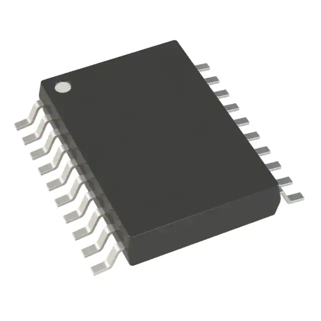
Analog Devices Inc. AD9833BRM-REEL7
- Part No.:
- AD9833BRM-REEL7
- Manufacturer:
- Analog Devices Inc.
- Category:
- Direct Digital Synthesis (DDS)
- Package:
- 10-TFSOP, 10-MSOP (0.118", 3.00mm Width)
- Datasheet:
-
 AD9833BRM-REEL7.pdf
- Description:
- IC DDS 25MHZ 10BIT 10MSOP
- Quantity:
- Payment:

- Shipping:

Inventory:4,828
Please send an inquiry. Send us your inquiry, and we will respond immediately.
Product details
Overview
AD9833BRM-REEL7 from Analog Devices is a low-power, 10-bit direct digital synthesis (DDS) waveform generator IC producing sine, triangular, and square wave outputs with 28-bit frequency resolution (0.1 Hz at 25 MHz MCLK), 12.5 MHz max output frequency, and 12.65 mW power consumption at 3 V. It operates from 2.3 V to 5.5 V, features a 3-wire SPI interface, and is used in TDR, flow measurement, and sensor excitation circuits.
For engineers reviewing the AD9833BRM-REEL7 datasheet, AD9833BRM-REEL7 pinout, AD9833BRM-REEL7 application, or AD9833BRM-REEL7 equivalent, key selection criteria include its 28-bit frequency tuning resolution, integrated 10-bit DAC with on-board 200 Ω load, MSOP-10 package, −40°C to +105°C automotive-grade operation, and sleep-mode current of 0.5 mA.
Technical Context
The AD9833BRM-REEL7 implements a 28-bit phase accumulator driving a 12-bit address SIN ROM, followed by a 10-bit current-source DAC. Its DDS architecture enables continuous-phase frequency switching without glitches via dual 28-bit frequency registers (FREQ0/FREQ1) and dual 12-bit phase registers (PHASE0/PHASE1).
Control is delivered through a 3-wire SPI-compatible serial interface (FSYNC, SCLK, SDATA) supporting up to 40 MHz SCLK, with register writes requiring 16-bit words and frame synchronization via active-low FSYNC. The device includes a programmable sleep function that powers down the DAC while maintaining MCLK operation.
Key Specifications
| Parameter | Value and Actual Design Meaning |
|---|---|
| Output Frequency Range | 0 MHz to 12.5 MHz - supports full-spectrum stimulus generation up to Nyquist limit of 25 MHz MCLK. |
| Frequency Resolution | 28-bit (0.1 Hz at 25 MHz MCLK) - enables precise calibration and fine-grained sweep control in metrology applications. |
| DAC Resolution | 10-bit - delivers 1,024 discrete amplitude steps for accurate waveform fidelity in sensor excitation. |
| Power Consumption | 12.65 mW at 3 V - allows battery-powered portable test equipment and low-energy embedded systems. |
| Supply Voltage Range | 2.3 V to 5.5 V - compatible with single-supply industrial microcontrollers and mixed-signal SoCs. |
| Operating Temperature | −40°C to +105°C - AEC-Q100 qualified for under-hood automotive sensing and industrial field instrumentation. |
| SPI Interface Speed | Up to 40 MHz SCLK - ensures rapid frequency/phase reconfiguration in real-time closed-loop systems. |
Pinout & Package
AD9833BRM-REEL7 is housed in a 10-lead MSOP package with exposed pad (thermal performance: θJA = 206°C/W). Pin functions are validated per Analog Devices Rev. G datasheet Figure 5 and Table 4.
| Pin/Terminal | Circuit Role | Design Meaning |
|---|---|---|
| COMP | DAC bias decoupling node | Requires 20 pF capacitor to AGND to stabilize internal DAC reference; critical for THD performance. |
| VDD | Main power supply input | Supplies both analog and digital sections; accepts 2.3–5.5 V; requires 0.1 µF + 10 µF decoupling to AGND. |
| CAP/2.5V | On-chip 2.5 V regulator output | Provides regulated 2.5 V to digital core when VDD > 2.7 V; bypassed to VDD if VDD ≤ 2.7 V. |
| DGND | Digital ground reference | Must be separated from AGND except at single-point star ground to minimize digital noise coupling. |
| MCLK | Master clock input | Determines output frequency accuracy and phase noise floor; accepts up to 25 MHz fundamental clock. |
| VOUT | Analog voltage output | Delivers 0.65 VPP sine/triangle/square waves; includes internal 200 Ω series resistor - no external load required. |
| AGND | Analog ground reference | Reference for DAC and analog circuitry; must be isolated from DGND except at system-level ground point. |
| FSYNC | Frame sync / chip select | Active-low enable for SPI writes; must be held low for entire 16-bit transfer; timing-critical setup/hold per t7/t8. |
| SCLK | Serial clock input | Clocks data on falling edge; supports up to 40 MHz; idle state must be high before FSYNC assertion. |
| SDATA | Serial data input | 16-bit word input (MSB first); carries register address and data; latched on SCLK falling edges. |
Key Features
| Feature | Design Value |
|---|---|
| No external components required | Integrated 200 Ω load resistor and on-chip 2.5 V regulator eliminate BOM count and layout complexity. |
| Three waveform outputs | Selectable sine, triangular, or square wave via MODE bit - enables multi-modal sensor excitation without external circuitry. |
| Power-down (SLEEP) mode | Reduces current to 0.5 mA by disabling DAC while preserving MCLK path - ideal for duty-cycled TDR bursts. |
| Continuous-phase frequency switching | 28-bit NCO with dual FREQ registers avoids output discontinuities during real-time frequency sweeps. |
| Automotive qualification | AEC-Q100 Grade 2 (−40°C to +105°C) - certified for engine control, brake sensors, and transmission monitoring. |
Applications
| Flow Measurement | Sensor Excitation |
|---|---|
Use Scenario: Ultrasonic time-of-flight liquid/gas flow meters requiring precise, stable frequency sources for transducer drive. IC Role / Device Role / Timing Role: Programmable waveform generator providing swept or fixed-frequency excitation to piezoelectric transducers. Use Value: 28-bit frequency resolution enables sub-Hz calibration granularity; low THD (−56 dBc) minimizes measurement error from harmonic distortion. | Use Scenario: Proximity and motion detection using capacitive or inductive sensing elements needing clean, variable-frequency stimulation. IC Role / Device Role / Timing Role: Low-noise analog signal source generating excitation waveforms for impedance-based sensing front-ends. Use Value: Integrated 10-bit DAC and on-board 200 Ω load ensure repeatable output amplitude; 12.65 mW power enables always-on sensing in energy-constrained nodes. |
| TDR Testing | Medical Instrumentation |
Use Scenario: Time-domain reflectometry for cable fault location and PCB trace integrity analysis requiring fast-rise step or pulse generation. IC Role / Device Role / Timing Role: High-speed waveform synthesizer producing calibrated square waves with controlled edge rates for reflection analysis. Use Value: 12.5 MHz output bandwidth supports sub-meter spatial resolution; sleep mode reduces average power during idle intervals between measurements. | Use Scenario: Portable diagnostic devices such as impedance plethysmographs or bioimpedance analyzers requiring compact, low-power signal sources. IC Role / Device Role / Timing Role: Precision analog stimulus generator delivering calibrated waveforms to biological tissue interfaces. Use Value: −40°C to +105°C operation supports clinical and field-deployable units; 0.1 Hz resolution enables adaptive frequency scanning across tissue dispersion models. |
Equivalent & Alternatives
The following parts are listed as comparable options for similar waveform generation applications.
| Alternative Part | Technical Difference | Application Difference | Selection Advice |
|---|---|---|---|
| AD9834BRUZ-REEL7 | Includes integrated 200 MHz PLL clock multiplier; supports up to 50 MHz MCLK; same 28-bit resolution and MSOP-10 package. | Enables higher output frequencies (up to 25 MHz) and improved phase noise at high fOUT; requires external loop filter components. | Choose AD9834BRUZ-REEL7 when MCLK < 25 MHz is unavailable and higher output bandwidth is needed. |
| Si5351A-B-GMR | 3-output I²C-programmable clock generator; no DAC or analog output; outputs CMOS/LVDS; 8 kHz–200 MHz range. | Designed for digital clock distribution, not analog waveform synthesis; lacks sine/triangle/square analog outputs and DAC functionality. | Choose Si5351A-B-GMR only for digital clock tree applications - not a functional substitute for analog stimulus generation. |
Compared with AD9833BRM-REEL7, AD9834BRUZ-REEL7 extends frequency capability via on-chip PLL but adds design complexity, while Si5351A-B-GMR provides multi-output digital clocks but cannot replace analog waveform synthesis - making AD9833BRM-REEL7 uniquely suited for low-power, self-contained analog excitation.
Availability
AD9833BRM-REEL7 is available at Aetrix Electronics and suitable for time-domain reflectometry, flow metering, and sensor excitation applications requiring stable component supply, long-term lifecycle support, and AEC-Q100-compliant performance.
Supply support for AD9833BRM-REEL7 includes scheduled delivery planning, volume procurement assistance, BOM continuity management, traceable sourcing, and lifecycle availability coordination for OEM customers, industrial embedded developers, connected-device designers, and electronics production programs.
Manufacturer
Analog Devices, Inc. is a global leader in high-performance analog, mixed-signal, and digital signal processing semiconductors, headquartered in Norwood, MA.
The AD983x series is designed specifically for low-power, programmable analog waveform generation in sensing, metrology, and test equipment - emphasizing integration, resolution, and temperature robustness over raw speed.
FAQ
What is the maximum output frequency supported by the AD9833BRM-REEL7?
The AD9833BRM-REEL7 supports a maximum output frequency of 12.5 MHz, limited by the Nyquist criterion relative to its 25 MHz maximum master clock (MCLK) input. This is confirmed in the General Description and Specifications sections of the Rev. G datasheet, where output frequency range is explicitly stated as 0 MHz to 12.5 MHz under all operating conditions.
Does the AD9833BRM-REEL7 require external passive components for basic operation?
No, the AD9833BRM-REEL7 requires no external passive components for core waveform generation. It integrates a 200 Ω output load resistor and an on-chip 2.5 V regulator. Only decoupling capacitors (0.1 µF + 10 µF on VDD–AGND; 100 nF on CAP/2.5V–DGND; 20 pF on COMP–AGND) are mandatory per the datasheet's Test Circuit (Figure 2) and Pin Descriptions.
How does the AD9833BRM-REEL7 achieve 28-bit frequency resolution with a 10-bit DAC?
The AD9833BRM-REEL7 achieves 28-bit frequency resolution via its numerically controlled oscillator (NCO), which uses a 28-bit phase accumulator to compute phase increments. The 10-bit DAC converts only the upper 10 bits of the 12-bit SIN ROM output - sufficient because phase truncation error is kept below DAC LSB weight by using two extra phase bits, as detailed in the Circuit Description section.
Is the AD9833BRM-REEL7 pin-compatible with other members of the AD983x family?
No, the AD9833BRM-REEL7 is not pin-compatible with AD9834 or AD9837. While all use 10-lead MSOP packages, pin assignments differ: AD9834 adds PLL-related pins (e.g., LOOPFLT), and AD9837 replaces FSYNC with a hardware RESET pin. The AD9833BRM-REEL7 pinout is unique to its 3-wire SPI interface and is defined exclusively in Figure 5 of the Rev. G datasheet.
What is the wake-up time from sleep mode for the AD9833BRM-REEL7?
The wake-up time from sleep mode for the AD9833BRM-REEL7 is 1 ms, as specified in the "LOGIC INPUTS" subsection of the Specifications table (Table 1) in the Rev. G datasheet. This value is measured from sleep exit command to valid analog output, and is guaranteed across the full −40°C to +105°C temperature range.
AD9833BRM-REEL7 Specifications
- Product attributes
- Attribute value
- Manufacturer:
- Analog Devices Inc.
- Series:
- -
- Package/Case:
- 10-TFSOP, 10-MSOP (0.118", 3.00mm Width)
- Packaging:
- Tape & Reel (TR)
- Product Status:
- Obsolete
- Resolution (Bits):
- 10 b
- Master fclk:
- 25 MHz
- Tuning Word Width (Bits):
- 28 b
- Voltage - Supply:
- 2.3V ~ 5.5V
- Operating Temperature:
- -40°C ~ 105°C
- Grade:
- -
- Qualification:
- -
- Mounting Type:
- Surface Mount
- Supplier Device Package:
- 10-MSOP
AD9833BRM-REEL7 FAQ
1.How can I place an order for AD9833BRM-REEL7 through Aetrix?
Please submit a Request for Quotation (RFQ) for AD9833BRM-REEL7 on Aetrix. Our sales agent will provide a competitive quotation and guide you through the order confirmation once you accept the terms.
2.Are the price and stock information for AD9833BRM-REEL7 reliable?
The price and inventory of AD9833BRM-REEL7 are updated periodically and may fluctuate due to market conditions. Stock and pricing data are typically refreshed every 24 hours. Quotation validity for AD9833BRM-REEL7 is usually 5 days.
3.What payment methods are accepted for AD9833BRM-REEL7?
We accept Wire Transfer, PayPal, Credit Card, Western Union, MoneyGram, and Escrow for AD9833BRM-REEL7 transactions.
Note: Certain payment methods may incur a processing fee.
4.How is shipping managed for AD9833BRM-REEL7?
AD9833BRM-REEL7 orders can be shipped via leading logistics carriers, including DHL, UPS, FedEx, TNT, or Registered Mail.
Once your AD9833BRM-REEL7 order is processed, you will receive an email with the shipment details and tracking number.
Note: Tracking information may take up to 24 hours to appear. Express delivery typically takes 3–5 business days.
5.How can I obtain technical support or documentation for AD9833BRM-REEL7?
For technical support, including AD9833BRM-REEL7 datasheets, pinout diagrams, or application guidance, please contact our engineering support team. They can provide detailed documentation and assistance for your AD9833BRM-REEL7 requirements.
6.How does Aetrix verify that AD9833BRM-REEL7 is sourced from the original manufacturer or authorized distributors?
All AD9833BRM-REEL7 products on Aetrix are procured from qualified distributors and authorized channels. Our dedicated quality assurance team conducts strict verification, including traceability checks and, if necessary, third-party testing. This ensures that AD9833BRM-REEL7 meets industry standards.
7.What is the process for return or replacement of AD9833BRM-REEL7?
All AD9833BRM-REEL7 units undergo pre-shipment inspection (PSI). If there is an issue with AD9833BRM-REEL7, returns or replacements are accepted under the following conditions:
1.Quantity discrepancies, incorrect items, or visible external defects (such as breakage or corrosion), acknowledged by Aetrix.
2.The issue is reported within 90 days of delivery.
3.The AD9833BRM-REEL7 part is unused and in its original packaging.
Return procedure for AD9833BRM-REEL7:
1.Submit a request within 90 days.
2.Obtain a Return Material Authorization (RMA) from Aetrix.
AD9833BRM-REEL7 Tags
-
AD9837ACPZ-RL
Analog Devices Inc.
-
AD9837ACPZ-RL7
Analog Devices Inc.
-
AD9837BCPZ-RL7
Analog Devices Inc.
-
AD9838BCPZ-RL7
Analog Devices Inc.
-
AD5932YRUZ
Analog Devices Inc.
-
AD9833BRMZ-REEL
Analog Devices Inc.
-
AD9833BRMZ-REEL7
Analog Devices Inc.
-
AD9833BRMZ
Analog Devices Inc.

-
AD9831ASTZ
Analog Devices Inc.
-
AD9834BRUZ-REEL7
Analog Devices Inc.
-
AD9834BRUZ
Analog Devices Inc.
-
AD9834CRUZ
Analog Devices Inc.
Tech Hub

A practical engineering guide to 3.3V and 5V logic compatibility, input thresholds, resistor dividers, translator ICs, MOSFET level shifting, I2C pull-ups, timing limits and power-sequencing risks.

The 74HC595 uses push-pull logic outputs, while the TPIC6B595 uses 50 V open-drain DMOS sinks for higher-power loads. This guide compares timing, current limits, 3.3 V interfacing, load wiring, thermal…

The 74HC595 converts serial data into eight stable parallel outputs. This guide covers pin functions, shift and storage timing, OE and MR behavior, drive-current limits, cascading, voltage compatibilit…

A technical comparison of level-sensitive latches and edge-triggered flip-flops, covering timing windows, setup and hold limits, master–slave operation, time borrowing, race-through, HDL inference and…

A D latch stores one bit while Enable controls when data can pass. This reference covers gate-level operation, truth tables, transparency, setup and hold timing, LE versus OE, common ICs and practical …

An SR latch stores one bit through cross-coupled feedback. This engineering reference covers NOR and NAND implementations, truth tables, forbidden-state recovery, gated operation, switch debouncing, fa…

Latch circuits retain one bit through feedback. This technical reference covers SR and D latches, truth tables, transparency, timing limits, latch-versus-flip-flop behavior, applications and common log…

An engineering guide to LED driver operation, constant-current and constant-voltage outputs, linear and switching topologies, dimming, IC selection, calculations, replacement compatibility, and fault c…

Operational amplifier guide covering op amp basics, feedback, ideal vs real op amps, common configurations, buffer circuits, offset, bias current, gain-bandwidth, slew rate, rail-to-rail limits and sel…

Jumper cables guide covering safe connection order, red and black clamp placement, final ground connection, cable gauge, length, clamp quality, copper vs CCA cables, jump starter comparison and battery…


