
 My Inquiry
 My Account


Analog Devices Inc. AD9853AS
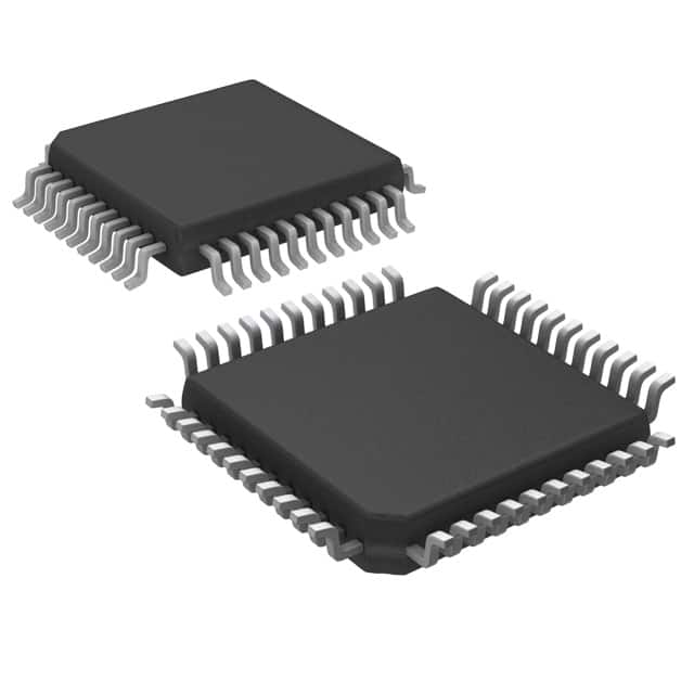
- Part No.:
- AD9853AS
- Manufacturer:
- Analog Devices Inc.
- Category:
- Direct Digital Synthesis (DDS)
- Package:
- 44-QFP
- Datasheet:
-
 AD9853AS.pdf
- Description:
- IC DGTL MODULATOR W/DAC 44-MQFP
- Quantity:
- Payment:

- Shipping:

Inventory:10,747
Please send an inquiry. Send us your inquiry, and we will respond immediately.
Product details
Overview
AD9853AS from Analog Devices is a programmable digital QPSK/16-QAM modulator IC integrating DDS, 10-bit DAC, dual CIC/FIR interpolation filters, Reed-Solomon FEC, and randomizer/preamble insertion - operating from –40°C to +85°C in MQFP-44 package. It delivers >50 dB SFDR at 42 MHz output, supports 5–42 MHz HFC return-channel transmission, and interfaces directly with AD8320 cable driver for complete upstream modem signal chain.
For engineers reviewing the AD9853AS datasheet, AD9853AS pinout, AD9853AS application, or AD9853AS equivalent, this page provides verified technical context, exact pin functions, modulation-specific timing constraints, real-world spectral performance (e.g., –44 dBm adjacent channel power at 30 MHz), and validated alternatives for HFC, DOCSIS, and wireless LAN return-path designs.
Technical Context
The AD9853AS implements a full digital modulation pipeline: serial data enters via DATA IN, passes through programmable R-S FEC (t = 0–10) and Davic/DVB/DOCSIS-compliant randomizer, then feeds a selectable FSK/QPSK/DQPSK/16-QAM/D16-QAM encoder. Output is shaped by a 41-tap linear-phase FIR filter and interpolated via two cascaded CIC stages (ICIC1 × ICIC2 × 4/M) before DAC conversion.
Its DDS core accepts 32-bit frequency tuning words and supports 6× reference clock multiplication (enabled/disabled via control bus). The analog output stage features complementary current-mode IOUT/IOUTB (5–20 mA full-scale), voltage compliance of –0.5 V to +1.5 V, and direct interface capability to AD8320 gain control bus - all powered from single +3.3 V or +5 V supply.
Key Specifications
| Parameter | Value and Actual Design Meaning |
|---|---|
| Modulation Formats | FSK, QPSK, DQPSK, 16-QAM, D16-QAM - selectable via control bus register 05h; enables interoperable HFC return-path compliance. |
| DAC Resolution & Output | 10-bit resolution; 5–20 mA full-scale current output (IOUT/IOUTB); supports external RSET resistor (3.9 kΩ typical) for gain calibration. |
| Reference Clock Range | +3.3 V: 7–21 MHz (6× enabled) or 42–126 MHz (6× disabled); determines max symbol rate and carrier frequency agility. |
| SFDR @ 42 MHz | 48–50 dBc (typical) - defines usable dynamic range for multi-carrier HFC upstream where in-band spurs must be suppressed ≥42 dBc. |
| FEC Capability | Reed-Solomon encoder with programmable t = 0–10, K = 16–255, N ≤ 255; primitive polynomial x⁸+x⁴+x³+x²+1; enables DOCSIS 1.0/1.1 forward error correction. |
| Power Consumption | 750 mW @ full clock speed (+3.3 V); drops to 16–20 mW with all power-down modes enabled - critical for burst-mode cable modem operation. |
| Output Carrier Range | DC–63 MHz (+3.3 V), DC–84 MHz (+5 V); covers full 5–42 MHz HFC upstream band and extends to 65 MHz for MMDS/WLAN. |
Pinout & Package
Metric Quad Flatpack (MQFP-44), S-44A package, surface-mount, lead-free compatible, θJA = 36°C/W.
| Pin/Terminal | Circuit Role | Design Meaning |
|---|---|---|
| REF CLK IN (Pin 38) | Reference clock input | Accepts 7–126 MHz CMOS-level clock; enables 6× internal PLL multiplication; duty cycle 40–60% required for stable lock. |
| DATA IN (Pin 41) | Serial baseband data input | Bit-synchronous input stream; sampled on rising edge of TXENABLE; requires exact sub-multiple relationship to REF CLK. |
| TXENABLE (Pin 42) | Burst framing control | Active-high pulse defining valid data window; minimum low time = preamble + 8 symbols; triggers 6-symbol data latency (tDL). |
| IOUT / IOUTB (Pins 24/25) | Differential DAC current outputs | Complementary 10-bit current sources; require external LP filter and termination (e.g., 50 Ω to AVDD/AGND) before AD8320 input. |
| FEC ENABLE (Pin 5) | Hardware FEC enable/disable | Logic high enables R-S encoding; logic low bypasses FEC block; zero hold time (tFH/tFL = 0 ns) allows dynamic on-the-fly control. |
| RESET (Pin 32) | Master asynchronous reset | Active-low; clears all control registers (including 48h defaulting to 63× REFCLK disabled), flushes FIR/CIC pipelines with zeros. |
| CONTROL BUS CLOCK / DATA IN (Pins 3/4) | Serial configuration interface | 25 MHz max I²C-compatible bus; 8-bit device address (000001XY) with X = Pin 6 voltage, Y = R/W bit; supports contiguous register writes. |
Key Features
| Feature | Design Value |
|---|---|
| Programmable 41-tap FIR filter | Linear-phase, 10-bit coefficient storage; fully loaded via control bus (Registers 1Eh–47h); enables precise α = 0.25 root-Nyquist pulse shaping per DOCSIS spec. |
| Dual cascaded CIC interpolators | Configurable ICIC1 (3–31) and ICIC2 (2–63); combined with fixed ×4 FIR interpolation and M-factor (2 for QPSK, 4 for 16-QAM) sets exact symbol-to-clock ratio. |
| DOCSIS/Davic-compliant randomizer | Selectable x⁶+x⁵+1 (Davic/DVB) or x¹⁵+x¹⁴+1 (DOCSIS) polynomials; programmable seed; transposable before/after FEC in signal chain. |
| Integrated preamble insertion | 0–96 bit length; programmable content (Registers 04h/11h); inserted prior to FEC/randomizer; cleared automatically on RESET assertion. |
| Direct AD8320 gain control | Register 49h outputs 8-bit gain control byte (GCB); sets AD8320 amplifier gain as AV = 0.316 + 0.077 × GCB (0–255 decimal); eliminates external DAC or GPIO control. |
Applications
| HFC Return-Path Modem | DOCSIS 1.x Upstream Transmitter |
|---|---|
Use Scenario: Bidirectional cable network upstream transmission in 5–42 MHz band with burst-mode TDMA access. IC Role / Device Role / Timing Role: Primary digital modulator generating QPSK/16-QAM carriers; handles FEC, randomization, pulse shaping, and interpolation before DAC output. Use Value: Meets DOCSIS 1.0/1.1 spectral mask requirements (≥42 dBc in-band spurs, –44 dBm adjacent channel power) while enabling compact, low-power chipset with AD8320. |
Use Scenario: Cable modem upstream PHY layer supporting 2.56 MS/s symbol rate and variable burst lengths per MAC protocol. IC Role / Device Role / Timing Role: Serial data framing engine synchronized to TXENABLE; manages R-S codeword boundaries (N = K + 2t), preamble alignment, and deterministic 6-symbol latency. Use Value: Guarantees bit-accurate, low-jitter modulation timing essential for upstream collision avoidance and ranging response windows. |
| Wireless LAN Baseband Modulator | MMDS Point-to-Multipoint Transmitter |
Use Scenario: 2.4 GHz ISM band WLAN base station transmitting QPSK/DQPSK signals with adaptive coding. IC Role / Device Role / Timing Role: Direct digital upconverter replacing analog mixers; generates baseband I/Q for quadrature upconversion; supports reconfigurable modulation on-the-fly. Use Value: Eliminates analog LO phase noise and image rejection issues; achieves >50 dB SFDR at 40 MHz AOUT for clean spectral occupancy. |
Use Scenario: Licensed 2.5 GHz MMDS infrastructure transmitter requiring 65 MHz carrier output and robust FEC for outdoor link reliability. IC Role / Device Role / Timing Role: High-frequency modulator operating at +5 V supply; uses 28 MHz REF CLK ×6 to generate 168 MHz system clock; drives AD8320 for +20 dBm RF output. Use Value: Enables full 65 MHz carrier generation (Fig. 12) with –42 dBc spurious emission - meeting FCC Part 101 spectral purity mandates. |
Equivalent & Alternatives
The following parts are listed as comparable options for similar digital modulator applications.
| Alternative Part | Technical Difference | Application Difference | Selection Advice |
|---|---|---|---|
| AD9854ASTZ | Successor IC with integrated 12-bit DAC, higher 300 MHz REF CLK support, and enhanced 1024-point programmable FIR; pinout incompatible (LQFP-80). | Targets next-gen DOCSIS 2.0/3.0 systems requiring higher SNR and wider bandwidth; not drop-in for AD9853AS PCBs. | Select AD9854ASTZ only when upgrading for >65 MHz carriers, improved SFDR (>60 dBc), or deeper FEC (t up to 16). |
| MAX2121ETJ+ | Dedicated QPSK/8PSK modulator with integrated PLL/VCO; no programmable FIR, no R-S FEC; 40-pin TQFN; operates up to 70 MHz carrier. | Used in satellite IF modulators and point-to-point radios; lacks cable-specific features (preamble, DOCSIS randomizer, AD8320 interface). | Choose MAX2121ETJ+ for cost-sensitive, fixed-modulation systems without FEC or programmable filtering requirements. |
Compared with AD9853AS, AD9854ASTZ offers higher resolution and flexibility but demands board redesign, while MAX2121ETJ+ simplifies design for non-cable applications but removes critical HFC features like R-S encoding and pulse-shaping control.
Availability
AD9853AS is available at Aetrix Electronics and suitable for HFC return-path modems, DOCSIS-compliant cable modems, and wireless LAN baseband transmitters requiring stable component supply across extended industrial temperature range (–40°C to +85°C).
Supply support for AD9853AS includes scheduled delivery planning, volume procurement assistance, BOM continuity management, traceable sourcing, and lifecycle availability coordination for OEM customers, industrial embedded developers, connected-device designers, and electronics production programs.
Manufacturer
Analog Devices, Inc. is a global leader in high-performance analog, mixed-signal, and digital signal processing semiconductors, headquartered in Norwood, MA.
The AD9853AS belongs to Analog Devices' broadband communications modulator product line, designed specifically for cost-effective, highly integrated upstream signal generation in hybrid fiber-coax (HFC) networks and wireless infrastructure.
FAQ
What modulation formats does the AD9853AS support, and how are they selected?
The AD9853AS supports FSK, QPSK, DQPSK, 16-QAM, and D16-QAM modulation formats. Selection is performed exclusively via Register 05h on the serial control bus: 000₂ = QPSK, 001₂ = DQPSK, 010₂ = 16-QAM, 011₂ = D16-QAM, and 100₂ = FSK. The AD9853AS does not support OQPSK or π/4-DQPSK; format changes require full register reconfiguration and RESET sequence.
Does the AD9853AS include an integrated PLL, and what reference clock frequencies does it accept?
Yes, the AD9853AS includes a 6× reference clock multiplier PLL (enabled/disabled via Register 48h bit 2). With +3.3 V supply, it accepts 7–21 MHz when 6× is enabled, or 42–126 MHz when disabled. With +5 V supply, the ranges are 18–28 MHz (6× enabled) or 108–168 MHz (6× disabled). The PLL locks to REF CLK IN (Pin 38) and drives the internal 165 MHz system clock.
How is the AD9853AS interfaced to the AD8320 cable driver amplifier?
The AD9853AS interfaces to the AD8320 via a dedicated 3-wire gain control bus (CA ENABLE, CA CLOCK, CA DATA - Pins 33–35). Writing an 8-bit value to Register 49h automatically formats and transmits the gain control byte (GCB) to AD8320, setting its gain as AV = 0.316 + 0.077 × GCB. No external microcontroller or level-shifting is required - the AD9853AS handles protocol translation and timing.
What is the data latency of the AD9853AS, and how does it affect burst-mode timing?
The AD9853AS exhibits a fixed data latency (tDL) of 6 symbols from TXENABLE assertion to valid AOUT waveform. This latency is deterministic and independent of interpolation rate or modulation format. In burst-mode TDMA systems, this must be accounted for in MAC-layer scheduling - e.g., a 64-symbol burst requires TXENABLE to be asserted 6 symbols before the first useful symbol appears at the output.
Can the AD9853AS operate with both +3.3 V and +5 V supplies, and how does supply voltage affect performance?
Yes, the AD9853AS is specified for single-supply operation from +3.3 V ±5% or +5 V ±5%. Supply voltage directly impacts maximum REF CLK frequency (126 MHz max at +3.3 V vs. 168 MHz at +5 V), carrier range (DC–63 MHz vs. DC–84 MHz), and power consumption (230 mA typ. at +3.3 V vs. 595 mA at +5 V). SFDR degrades slightly at higher frequencies under +3.3 V due to reduced headroom.
AD9853AS Specifications
- Product attributes
- Attribute value
- Manufacturer:
- Analog Devices Inc.
- Series:
- -
- Package/Case:
- 44-QFP
- Packaging:
- Bag
- Product Status:
- Obsolete
- Resolution (Bits):
- 10 b
- Master fclk:
- 165 MHz
- Tuning Word Width (Bits):
- 32 b
- Voltage - Supply:
- 3.3V, 5V
- Operating Temperature:
- -40°C ~ 85°C
- Grade:
- -
- Qualification:
- -
- Mounting Type:
- Surface Mount
- Supplier Device Package:
- 44-MQFP (10x10)
AD9853AS FAQ
1.How can I place an order for AD9853AS through Aetrix?
Please submit a Request for Quotation (RFQ) for AD9853AS on Aetrix. Our sales agent will provide a competitive quotation and guide you through the order confirmation once you accept the terms.
2.Are the price and stock information for AD9853AS reliable?
The price and inventory of AD9853AS are updated periodically and may fluctuate due to market conditions. Stock and pricing data are typically refreshed every 24 hours. Quotation validity for AD9853AS is usually 5 days.
3.What payment methods are accepted for AD9853AS?
We accept Wire Transfer, PayPal, Credit Card, Western Union, MoneyGram, and Escrow for AD9853AS transactions.
Note: Certain payment methods may incur a processing fee.
4.How is shipping managed for AD9853AS?
AD9853AS orders can be shipped via leading logistics carriers, including DHL, UPS, FedEx, TNT, or Registered Mail.
Once your AD9853AS order is processed, you will receive an email with the shipment details and tracking number.
Note: Tracking information may take up to 24 hours to appear. Express delivery typically takes 3–5 business days.
5.How can I obtain technical support or documentation for AD9853AS?
For technical support, including AD9853AS datasheets, pinout diagrams, or application guidance, please contact our engineering support team. They can provide detailed documentation and assistance for your AD9853AS requirements.
6.How does Aetrix verify that AD9853AS is sourced from the original manufacturer or authorized distributors?
All AD9853AS products on Aetrix are procured from qualified distributors and authorized channels. Our dedicated quality assurance team conducts strict verification, including traceability checks and, if necessary, third-party testing. This ensures that AD9853AS meets industry standards.
7.What is the process for return or replacement of AD9853AS?
All AD9853AS units undergo pre-shipment inspection (PSI). If there is an issue with AD9853AS, returns or replacements are accepted under the following conditions:
1.Quantity discrepancies, incorrect items, or visible external defects (such as breakage or corrosion), acknowledged by Aetrix.
2.The issue is reported within 90 days of delivery.
3.The AD9853AS part is unused and in its original packaging.
Return procedure for AD9853AS:
1.Submit a request within 90 days.
2.Obtain a Return Material Authorization (RMA) from Aetrix.
AD9853AS Tags
-
AD9837ACPZ-RL
Analog Devices Inc.
-
AD9837ACPZ-RL7
Analog Devices Inc.
-
AD9837BCPZ-RL7
Analog Devices Inc.
-
AD9838BCPZ-RL7
Analog Devices Inc.
-
AD5932YRUZ
Analog Devices Inc.
-
AD9833BRMZ-REEL
Analog Devices Inc.
-
AD9833BRMZ-REEL7
Analog Devices Inc.
-
AD9833BRMZ
Analog Devices Inc.

-
AD9831ASTZ
Analog Devices Inc.
-
AD9834BRUZ-REEL7
Analog Devices Inc.
-
AD9834BRUZ
Analog Devices Inc.
-
AD9834CRUZ
Analog Devices Inc.
Tech Hub

A practical engineering guide to 3.3V and 5V logic compatibility, input thresholds, resistor dividers, translator ICs, MOSFET level shifting, I2C pull-ups, timing limits and power-sequencing risks.

The 74HC595 uses push-pull logic outputs, while the TPIC6B595 uses 50 V open-drain DMOS sinks for higher-power loads. This guide compares timing, current limits, 3.3 V interfacing, load wiring, thermal…

The 74HC595 converts serial data into eight stable parallel outputs. This guide covers pin functions, shift and storage timing, OE and MR behavior, drive-current limits, cascading, voltage compatibilit…

A technical comparison of level-sensitive latches and edge-triggered flip-flops, covering timing windows, setup and hold limits, master–slave operation, time borrowing, race-through, HDL inference and…

A D latch stores one bit while Enable controls when data can pass. This reference covers gate-level operation, truth tables, transparency, setup and hold timing, LE versus OE, common ICs and practical …

An SR latch stores one bit through cross-coupled feedback. This engineering reference covers NOR and NAND implementations, truth tables, forbidden-state recovery, gated operation, switch debouncing, fa…

Latch circuits retain one bit through feedback. This technical reference covers SR and D latches, truth tables, transparency, timing limits, latch-versus-flip-flop behavior, applications and common log…

An engineering guide to LED driver operation, constant-current and constant-voltage outputs, linear and switching topologies, dimming, IC selection, calculations, replacement compatibility, and fault c…

Operational amplifier guide covering op amp basics, feedback, ideal vs real op amps, common configurations, buffer circuits, offset, bias current, gain-bandwidth, slew rate, rail-to-rail limits and sel…

Jumper cables guide covering safe connection order, red and black clamp placement, final ground connection, cable gauge, length, clamp quality, copper vs CCA cables, jump starter comparison and battery…


