
 My Inquiry
 My Account


Analog Devices Inc. AD9862BST
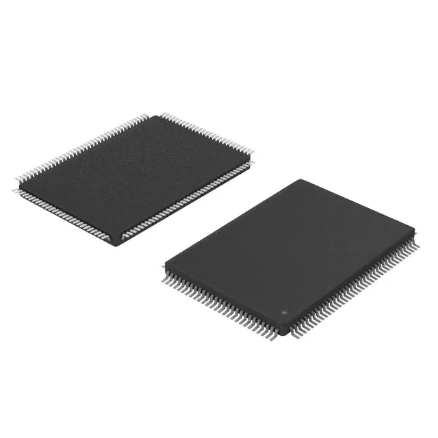
- Part No.:
- AD9862BST
- Manufacturer:
- Analog Devices Inc.
- Category:
- RF Front End (LNA + PA)
- Package:
- 128-LQFP
- Datasheet:
-
 AD9862BST.pdf
- Description:
- IC FRONT-END MIXED-SGNL 128-LQFP
- Quantity:
- Payment:

- Shipping:

Inventory:1,030
Please send an inquiry. Send us your inquiry, and we will respond immediately.
Product details
Overview
AD9862BST from Analog Devices is a 12-bit ADC / 14-bit DAC mixed-signal front-end (MxFE™) processor for broadband communications, featuring dual-channel receive and transmit paths, 64 MSPS ADC sampling, 128 MSPS DAC update rate, and integrated programmable gain amplifiers, Hilbert filters, and delay-locked loop clock generation. It serves as the core signal conditioning and conversion engine in cable modems and VDSL systems.
For engineers reviewing the AD9862BST datasheet, AD9862BST pinout, AD9862BST application, or AD9862BST equivalent, key selection considerations include its 12/14-bit resolution trade-off versus AD9860BST, Rx/Tx channel isolation >90 dB, 128-lead LQFP package compatibility, and support for real/I/Q baseband or low-IF architectures in fixed wireless and wireline infrastructure.
Technical Context
The AD9862BST implements a dual-path MxFE architecture with independent Rx and Tx signal chains. Each Rx channel integrates a 12-bit, 64 MSPS ADC, input buffer, 20 dB RxPGA, decimation filter, and bypassable digital Hilbert filter; each Tx channel includes a 14-bit, 128 MSPS current-output DAC, TxPGA with 20 dB range, interpolation filters (×2/×4), and digitally tunable quadrature mixers.
Timing is synchronized via an on-chip DLL clock multiplier supporting single-crystal or external clock inputs, generating internal clocks up to 128 MHz and two programmable external outputs (CLKOUT1/CLKOUT2). Device configuration uses a 3-wire SPI interface controlling over 100 registers, including auxiliary 10-bit ADCs and 8-bit DACs.
Key Specifications
| Parameter | Value and Actual Design Meaning |
|---|---|
| ADC Resolution | 12-bit - Enables high-fidelity digitization of analog IF/baseband signals with ≥64.75 dB SNDR at 5 MHz input. |
| DAC Resolution | 14-bit - Delivers fine-grained analog output control with ≤±3 LSB INL and 20 mA full-scale current scalability. |
| Max ADC Sampling Rate | 64 MSPS - Supports Nyquist sampling of signals up to 32 MHz bandwidth in standard timing mode. |
| Max DAC Update Rate | 128 MSPS - Enables direct synthesis of wideband signals (e.g., OFDM carriers) without external interpolation. |
| Rx Channel Isolation | >80 dB - Ensures minimal crosstalk between A/B receive channels during diversity or I/Q processing. |
| Tx-to-Rx Isolation | >90 dB - Prevents transmit leakage from saturating receiver front-end in half-duplex FDD systems. |
| Operating Temperature | –40°C to +70°C - Qualified for industrial-grade deployment in outdoor CPE and DSLAM line cards. |
| Package | 128-lead LQFP (ST-128B) - Standard surface-mount footprint with 0.4 mm pitch, compatible with automated assembly. |
Pinout & Package
AD9862BST is housed in a 128-lead Low Profile Plastic Quad Flatpack (LQFP), ST-128B package, with exposed thermal pad (not electrically connected). Pin functions are validated per Analog Devices' official pin configuration diagram and function descriptions (Rev. 0).
| Pin/Terminal | Circuit Role | Design Meaning |
|---|---|---|
| IOUT+A / IOUT–A | Differential current output (Channel A) | High-speed 14-bit DAC output pair requiring external termination (typically 50 Ω) and reconstruction filtering. |
| VIN+A / VIN–A | Differential analog input (Channel A) | 12-bit ADC input pair with 200 Ω differential impedance and 140 MHz –3 dB bandwidth. |
| D0A–D9A / D11A | Parallel ADC data bus (Channel A) | 12-bit parallel output (MSB-first) synchronized to RxSYNC; supports multiplexed or interleaved interface modes. |
| Tx0–Tx11 / Tx13 | Parallel DAC data bus (Channel A) | 14-bit parallel input (MSB-first) synchronized to TxSYNC; supports real or I/Q interleaving per timing mode. |
| RxSYNC / TxSYNC | Receive/Transmit frame sync | Asynchronous edge-triggered strobes defining data validity windows for parallel ADC/DAC interfaces. |
| OSC1 / OSC2 | Clock/crystal input | Differential crystal oscillator input pins enabling single-ended or crystal-based clock source with DLL multiplication. |
| CLKOUT1 / CLKOUT2 | Programmable clock outputs | Two buffered clocks derived from DLL; CLKOUT1 configurable as ×1 or ×2, CLKOUT2 as ×1/×2/×4 of reference. |
| SEN / SCLK / SDIO | SPI serial interface | 3-wire SPI port (enable, clock, bidirectional data) for register configuration, operating up to 16 MHz. |
Key Features
| Feature | Design Value |
|---|---|
| Dual 12-bit ADCs with RxPGA | 20 dB programmable gain range per channel enables dynamic signal level adaptation without external amplification. |
| Dual 14-bit DACs with TxPGA | 20 dB output current scaling allows precise RF power control across varying line impedances and modulation schemes. |
| Bypassable digital Hilbert filters | Enables flexible I/Q generation or correction in both Rx and Tx paths without hardware modification. |
| Interpolation filters (×2/×4) | Reduces external reconstruction filter complexity by lowering required stop-band attenuation by 12–24 dB. |
| Integrated DLL clock multiplier | Eliminates need for multiple external clock sources; supports single 32/64/128 MHz crystal or clock input. |
| Auxiliary 10-bit ADC & 8-bit DAC | Provides on-chip monitoring/control capability for system calibration, temperature sensing, or bias adjustment. |
Applications
| Cable Modem Front-End | VDSL Line Card Transceiver |
|---|---|
Use Scenario: Digitizing downstream QAM signals and reconstructing upstream TDMA bursts in DOCSIS-compliant cable modems. IC Role / Device Role / Timing Role: Dual-channel MxFE performing simultaneous 64 MSPS ADC sampling and 128 MSPS DAC synthesis with precise symbol timing alignment. Use Value: Integrated RxPGA and TxPGA eliminate discrete gain stages; >90 dB Tx-to-Rx isolation prevents self-interference during burst transmission. | Use Scenario: Full-duplex analog signal conditioning in VDSL2 line cards handling up to 30 MHz upstream/downstream bandwidth. IC Role / Device Role / Timing Role: High-linearity mixed-signal interface converting multi-tone DMT symbols between digital baseband and analog line drivers/receivers. Use Value: 12/14-bit resolution and >77 dB SFDR at 5 MHz enable compliance with ITU-T G.993.2 spectral mask requirements. |
| Fixed Wireless Access Baseband | MMDS/LMDS Subscriber Unit |
Use Scenario: Baseband processing in point-to-multipoint wireless access nodes using OFDM or QPSK modulation in 2.5–3.7 GHz bands. IC Role / Device Role / Timing Role: Real-time I/Q data path with programmable Hilbert filters and digital up/down-conversion for image rejection. Use Value: Bypassable Hilbert filters and ×4 interpolation allow flexible waveform generation without changing PCB layout or firmware. | Use Scenario: Compact subscriber terminal supporting 64-QAM in licensed MMDS spectrum, requiring low-power, high-dynamic-range signal conversion. IC Role / Device Role / Timing Role: Low-power MxFE operating in 32 MSPS mode with Rx buffer bypassed and 1V p-p input for optimized THD/SFDR trade-off. Use Value: Configurable low-power modes reduce Rx path current to 155 mA (32 MSPS) or 80 mA (16 MSPS), extending thermal margin in sealed enclosures. |
Equivalent & Alternatives
The following parts are listed as comparable options for similar mixed-signal front-end applications.
| Alternative Part | Technical Difference | Application Difference | Selection Advice |
|---|---|---|---|
| AD9860BST | 10-bit ADC / 12-bit DAC; lower SNR (60.66 dB) and SNDR (58.0 dB) at 5 MHz; identical pinout and package. | Targeted at cost-sensitive, lower-performance broadband modems where 12/14-bit resolution is not required. | Select AD9860BST when system-level SFDR >70 dBc and SNDR >58 dB are sufficient and BOM cost reduction is prioritized. |
| AD9961BCPZ | 10-/12-bit ADC / 10-/12-bit DAC; lower max DAC rate (80 MSPS); integrated PLL instead of DLL; 72-lead LFCSP package. | Designed for portable/wireless infrastructure with smaller footprint and lower power; lacks auxiliary ADC/DAC and Hilbert filter bypass. | Choose AD9961BCPZ only if space-constrained designs accept reduced dynamic range and loss of Hilbert flexibility. |
Compared with AD9860BST and AD9961BCPZ, AD9862BST delivers superior dynamic performance (72.0 dB SNR, 69.8 dB SNDR) and greater signal chain flexibility via programmable Hilbert filters and ×4 interpolation-critical for high-order QAM and OFDM in next-generation wireline systems.
Availability
AD9862BST is available at Aetrix Electronics and suitable for cable modems, VDSL line cards, and fixed wireless access equipment requiring stable component supply, long-term lifecycle support, and guaranteed industrial temperature operation.
Supply support for AD9862BST includes scheduled delivery planning, volume procurement assistance, BOM continuity management, traceable sourcing, and lifecycle availability coordination for OEM customers, industrial embedded developers, connected-device designers, and electronics production programs.
Manufacturer
Analog Devices, Inc. is a global leader in high-performance analog, mixed-signal, and digital signal processing semiconductors, headquartered in Norwood, MA.
The AD9862BST belongs to the MxFE™ (Mixed-Signal Front-End) product line, engineered specifically for broadband communication infrastructure requiring tightly integrated, high-dynamic-range ADC/DAC functionality with programmable signal conditioning.
FAQ
What is the maximum sampling rate supported by the AD9862BST ADC?
The AD9862BST supports a maximum ADC sampling rate of 64 MSPS in normal timing mode. This rate is maintained across both receive channels simultaneously and is specified under conditions of VA = 3.3 V ±5%, VD = 3.3 V ±10%, and fADC = 64 MHz. The device also supports lower rates (32 MSPS, 16 MSPS) in low-power modes to reduce current consumption while retaining 12-bit resolution.
Does the AD9862BST support I/Q signal processing in both receive and transmit paths?
Yes, the AD9862BST supports full I/Q signal processing in both paths. Its digital Hilbert filters are independently configurable and bypassable in Rx and Tx chains, enabling complex baseband generation and image-reject demodulation. The Tx path includes digitally tunable quadrature mixers, and the Rx path accepts real, diversity, or I/Q data at baseband or low IF-verified in the functional block diagram and timing specifications.
What is the purpose of the FSADJ pin on the AD9862BST?
The FSADJ pin on the AD9862BST is used to adjust the full-scale output current of the 14-bit DACs. By connecting an external resistor between FSADJ and AGND, users can scale the nominal 20 mA full-scale current output linearly-enabling precise matching to external reconstruction filter and driver stage requirements without modifying the DAC's digital gain control.
Can the AD9862BST operate with a single crystal oscillator input?
Yes, the AD9862BST can operate with a single crystal oscillator input applied to the OSC1 pin (with OSC2 grounded or left floating per design guidelines). Its integrated delay-locked loop (DLL) multiplies the crystal frequency to generate all internal clocks-including 128 MHz for DAC operation-and provides two programmable external clock outputs (CLKOUT1, CLKOUT2), eliminating the need for multiple clock sources.
How many auxiliary analog inputs and outputs does the AD9862BST provide?
The AD9862BST provides four auxiliary ADC inputs (AUX_ADC_A1, AUX_ADC_A2, AUX_ADC_B1, AUX_ADC_B2) and three auxiliary DAC outputs (AUX_DAC_A, AUX_DAC_B, AUX_DAC_C). The auxiliary ADC is 10-bit with 1.25 MSPS conversion rate and 3 V input range; the auxiliary DACs are 8-bit with 3 V output range and 8 µs settling time-fully documented in the "Auxiliary ADC" and "Auxiliary DAC" sections of the datasheet.
AD9862BST Specifications
- Product attributes
- Attribute value
- Manufacturer:
- Analog Devices Inc.
- Series:
- -
- Packaging:
- Bag
- Product Status:
- Obsolete
- RF Type:
- LMDS, MMDS
- Frequency:
- -
- Features:
- 12-Bit ADC(s), 14-Bit DAC(s)
- Grade:
- -
- Qualification:
- -
- Supplier Device Package:
- 128-LQFP (14x20)
AD9862BST FAQ
1.How can I place an order for AD9862BST through Aetrix?
Please submit a Request for Quotation (RFQ) for AD9862BST on Aetrix. Our sales agent will provide a competitive quotation and guide you through the order confirmation once you accept the terms.
2.Are the price and stock information for AD9862BST reliable?
The price and inventory of AD9862BST are updated periodically and may fluctuate due to market conditions. Stock and pricing data are typically refreshed every 24 hours. Quotation validity for AD9862BST is usually 5 days.
3.What payment methods are accepted for AD9862BST?
We accept Wire Transfer, PayPal, Credit Card, Western Union, MoneyGram, and Escrow for AD9862BST transactions.
Note: Certain payment methods may incur a processing fee.
4.How is shipping managed for AD9862BST?
AD9862BST orders can be shipped via leading logistics carriers, including DHL, UPS, FedEx, TNT, or Registered Mail.
Once your AD9862BST order is processed, you will receive an email with the shipment details and tracking number.
Note: Tracking information may take up to 24 hours to appear. Express delivery typically takes 3–5 business days.
5.How can I obtain technical support or documentation for AD9862BST?
For technical support, including AD9862BST datasheets, pinout diagrams, or application guidance, please contact our engineering support team. They can provide detailed documentation and assistance for your AD9862BST requirements.
6.How does Aetrix verify that AD9862BST is sourced from the original manufacturer or authorized distributors?
All AD9862BST products on Aetrix are procured from qualified distributors and authorized channels. Our dedicated quality assurance team conducts strict verification, including traceability checks and, if necessary, third-party testing. This ensures that AD9862BST meets industry standards.
7.What is the process for return or replacement of AD9862BST?
All AD9862BST units undergo pre-shipment inspection (PSI). If there is an issue with AD9862BST, returns or replacements are accepted under the following conditions:
1.Quantity discrepancies, incorrect items, or visible external defects (such as breakage or corrosion), acknowledged by Aetrix.
2.The issue is reported within 90 days of delivery.
3.The AD9862BST part is unused and in its original packaging.
Return procedure for AD9862BST:
1.Submit a request within 90 days.
2.Obtain a Return Material Authorization (RMA) from Aetrix.
AD9862BST Tags
-
RFX2401C
Skyworks Solutions Inc.
.jpg)
-
NRF21540-QDAA-R
Nordic Semiconductor ASA
-
NRF21540-QDAA-R7
Nordic Semiconductor ASA
-
RFX2411N
Skyworks Solutions Inc.
-
SE2438T-R
Skyworks Solutions Inc.
-
SKY66118-11
Skyworks Solutions Inc.
-
SKY85712-21
Skyworks Solutions Inc.

-
SKY85329-11
Skyworks Solutions Inc.
-
SKY66422-11
Skyworks Solutions Inc.

-
SKY66119-11
Skyworks Solutions Inc.
-
NJG1156PCD-TE1
Nisshinbo Micro Devices Inc.
-
SE2435L-R
Skyworks Solutions Inc.
Tech Hub

A practical engineering guide to 3.3V and 5V logic compatibility, input thresholds, resistor dividers, translator ICs, MOSFET level shifting, I2C pull-ups, timing limits and power-sequencing risks.

The 74HC595 uses push-pull logic outputs, while the TPIC6B595 uses 50 V open-drain DMOS sinks for higher-power loads. This guide compares timing, current limits, 3.3 V interfacing, load wiring, thermal…

The 74HC595 converts serial data into eight stable parallel outputs. This guide covers pin functions, shift and storage timing, OE and MR behavior, drive-current limits, cascading, voltage compatibilit…

A technical comparison of level-sensitive latches and edge-triggered flip-flops, covering timing windows, setup and hold limits, master–slave operation, time borrowing, race-through, HDL inference and…

A D latch stores one bit while Enable controls when data can pass. This reference covers gate-level operation, truth tables, transparency, setup and hold timing, LE versus OE, common ICs and practical …

An SR latch stores one bit through cross-coupled feedback. This engineering reference covers NOR and NAND implementations, truth tables, forbidden-state recovery, gated operation, switch debouncing, fa…

Latch circuits retain one bit through feedback. This technical reference covers SR and D latches, truth tables, transparency, timing limits, latch-versus-flip-flop behavior, applications and common log…

An engineering guide to LED driver operation, constant-current and constant-voltage outputs, linear and switching topologies, dimming, IC selection, calculations, replacement compatibility, and fault c…

Operational amplifier guide covering op amp basics, feedback, ideal vs real op amps, common configurations, buffer circuits, offset, bias current, gain-bandwidth, slew rate, rail-to-rail limits and sel…

Jumper cables guide covering safe connection order, red and black clamp placement, final ground connection, cable gauge, length, clamp quality, copper vs CCA cables, jump starter comparison and battery…


