
 My Inquiry
 My Account


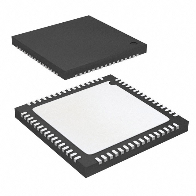
Analog Devices Inc. AD9866BCP
- Part No.:
- AD9866BCP
- Manufacturer:
- Analog Devices Inc.
- Category:
- RF Front End (LNA + PA)
- Package:
- 64-VFQFN Exposed Pad, CSP
- Datasheet:
-
 AD9866BCP.pdf
- Description:
- IC FRONT-END MIXED-SGNL 64-LFCSP
- Quantity:
- Payment:

- Shipping:

Inventory:2,352
Please send an inquiry. Send us your inquiry, and we will respond immediately.
Product details
Overview
AD9866 from Analog Devices is a 3.3 V CMOS mixed-signal front-end (MxFE®) IC for broadband modem transceivers, integrating a 12-bit 200 MSPS DAC with 2×/4× interpolation, a 12-bit 80 MSPS ADC, programmable RxPGA (−12 dB to +48 dB), third-order LPF (15–35 MHz), and integrated 23 dBm line driver with 19.5 dB digital gain control - deployed in powerline networking and VDSL systems.
For engineers reviewing the AD9866 datasheet, AD9866 pinout, AD9866 application, or AD9866 equivalent, key selection considerations include full-duplex/half-duplex interface flexibility, Tx-to-Rx isolation up to 123 dBc, SPI-programmable gain/PLL/clock outputs, and LFCSP-64 package thermal performance with exposed pad grounding.
Technical Context
The AD9866 implements a dual-path transceiver architecture: the transmit path combines a bypassable 2×/4× digital interpolation filter, 12-bit TxDAC with differential current outputs (IOUT_P±), and a configurable IAMP line driver supporting both current- and voltage-mode operation delivering >23 dBm peak power. The receive path integrates a low-noise RxPGA (<2.5 nV/√Hz at high gain), tunable third-order LPF, and pipeline ADC with scalable power consumption.
Digital control is handled via a 32 MHz SPI interface managing register-mapped blocks including RxPGA gain (1 dB steps), Tx gain (0.5 dB steps), LPF cutoff, clock multiplier PLL (5–80 MHz OSCIN input), and two auxiliary clock outputs (CLKOUT1/CLKOUT2) with jitter as low as 6 ps rms. Power management supports per-block power-down and half-duplex mode optimization.
Key Specifications
| Parameter | Value and Actual Design Meaning |
|---|---|
| DAC Resolution | 12-bit, enabling 4096 discrete output levels for high-fidelity signal synthesis in VDSL upstream channels. |
| DAC Update Rate | 200 MSPS, supporting baseband signal generation up to 34 MHz bandwidth with 4× interpolation. |
| ADC Resolution | 12-bit, providing 72 dB theoretical SNR for accurate digitization of received analog signals. |
| ADC Sampling Rate | 5–80 MSPS, allowing flexible data rate adaptation across HPNA, VDSL, and powerline PHY layers. |
| RxPGA Gain Range | −12 dB to +48 dB in 1 dB steps, permitting dynamic range adjustment to match varying line signal amplitudes. |
| Tx Line Driver Output | ≥23 dBm peak power, meeting spectral mask and output level requirements for Class A/B VDSL line drivers. |
| Full-Duplex Isolation | Up to 123 dBc (IOUTP± to RX±, 0 dB RxPGA gain), minimizing Tx leakage into Rx path during simultaneous operation. |
| Package | 64-lead LFCSP (CP-64-31), with exposed thermal pad requiring soldering to PCB ground plane for θJA = 23.3°C/W. |
Pinout & Package
AD9866 is housed in a 64-lead lead frame chip scale package (LFCSP, CP-64-31) with an exposed thermal pad that must be soldered to the PCB ground plane for thermal and electrical integrity. Pin 1 identifier is marked; all AVSS/DRVSS/CLKVSS pins are dedicated ground returns.
| Pin/Terminal | Circuit Role | Design Meaning |
|---|---|---|
| IOUT_P+/IOUT_P− | TxDAC Differential Current Outputs | Source current outputs for direct connection to external load or internal IAMP; define DAC full-scale current (2–25 mA). |
| IOUT_N+/IOUT_N− | Mirror Current Outputs (IAMP) | Sink current paths for IAMP's current-mode line driver configuration; support ≥80 mA full-scale. |
| IOUT_G+/IOUT_G− | Amp Current Outputs (IAMP) | Sink current paths for IAMP's voltage-mode line driver (with external NPN transistors); support ≥105 mA full-scale. |
| RX+/RX− | Differential ADC Inputs | High-impedance (400 Ω || 4 pF) inputs accepting 8 mVp-p to 6.33 Vp-p based on RxPGA gain setting. |
| ADIO[11:0] | Half-/Full-Duplex Data Bus | Configurable 12-bit bidirectional port: HD mode uses ADIO[11:0] as parallel buffer; FD mode splits into Tx[5:0]/Rx[5:0]. |
| TXEN/TXSYNC & RXEN/RXSYNC | Interface Control Signals | Enable/synchronize Tx and Rx data transfers; support independent timing in half-duplex or aligned strobing in full-duplex. |
| SCLK/SDIO/SEN | SPI Serial Interface | 32 MHz max SCLK; SDIO bidirectional; SEN active-low enables register access; supports daisy-chain configuration. |
| CLKOUT1/CLKOUT2 | Programmable Clock Outputs | CLKOUT1 derived from fDAC/N (N=1,2,4,8); CLKOUT2 is inverted OSCIN replica; jitter ≤12 ps rms (CLKOUT1), ≤6 ps rms (CLKOUT2). |
Key Features
| Feature | Design Value |
|---|---|
| Integrated Tx/Rx signal chain | Replaces discrete ADC+DAC+PGA+filter+driver solutions, reducing BOM count and board area in modem designs. |
| Backward compatibility | Pin- and register-compatible with AD9975 and AD9876, enabling drop-in upgrades without layout changes. |
| Flexible digital interface | Supports half-duplex (12-bit ADIO bus) and full-duplex (separate Tx[5:0]/Rx[5:0]) modes, simplifying integration with FPGA/DSP back ends. |
| Low-noise RxPGA | Input-referred noise <2.5 nV/√Hz at +48 dB gain ensures high sensitivity for weak-line VDSL reception. |
| On-chip PLL & clock synthesis | Generates all internal clocks (fDAC, fADC, fCLKOUT) from single 5–80 MHz crystal or clock source, eliminating external clock ICs. |
| Scalable power architecture | Per-block power-down (e.g., disable IAMP in Rx-only mode) reduces total supply current from 475 mA (full-duplex) to 13 mA (standby). |
Applications
| Powerline Networking | VDSL Transceivers |
|---|---|
Use Scenario: High-speed data transmission over existing AC power wiring in smart grid and home networking applications. IC Role / Device Role / Timing Role: MxFE transceiver handling physical layer modulation/demodulation, with Tx path generating OFDM symbols and Rx path digitizing attenuated, noisy line signals. Use Value: Integrated 23 dBm line driver meets EN 50561-1 spectral emission limits; programmable LPF rejects out-of-band switching noise from SMPS on same board. | Use Scenario: Customer-premises equipment (CPE) and DSLAM line cards operating in VDSL2 Annex A/M profiles up to 30 MHz. IC Role / Device Role / Timing Role: Full-duplex analog front end converting multi-tone QAM signals between digital baseband and twisted-pair copper medium. Use Value: 123 dBc Tx-to-Rx isolation prevents near-end crosstalk; 80 MSPS ADC supports 21 MHz usable bandwidth per VDSL2 profile. |
| HPNA 3.1 Systems | Broadband Modem Reference Designs |
Use Scenario: Home phoneline networking adapters coexisting with POTS and ADSL on shared telephone lines. IC Role / Device Role / Timing Role: Mixed-signal interface managing time-division duplex (TDD) operation, with fast RxPGA gain settling (20 ns for 5 dB step) enabling rapid AGC response. Use Value: Half-duplex power savings reduce idle current to 39 mA (Rx mode), extending thermal margin in compact enclosures. | Use Scenario: Evaluation and production platforms for cable, DSL, and fiber access gateways requiring rapid prototyping. IC Role / Device Role / Timing Role: Reference MxFE enabling validation of PHY firmware, clock tree design, and RF front-end matching networks. Use Value: SPI-configurable registers and dual clock outputs simplify timing verification; LFCSP package supports high-density layout with controlled impedance routing. |
Equivalent & Alternatives
The following parts are listed as comparable options for similar mixed-signal transceiver applications.
| Alternative Part | Technical Difference | Application Difference | Selection Advice |
|---|---|---|---|
| AD9867BCP | Same architecture but adds 10-bit auxiliary DAC and enhanced AGC logic; higher IDD in full-duplex mode (510 mA vs. 475 mA). | Targeted at next-gen VDSL2+ and G.fast where dynamic AGC headroom and auxiliary signaling are required. | Select AD9867BCP only if auxiliary DAC or tighter AGC loop latency is needed; AD9866 remains optimal for cost-sensitive VDSL2 deployments. |
| MAX2986ETM+ | 10-bit DAC/ADC, lower Tx output (18 dBm), no integrated PLL; requires external clock generator and separate PGA/filter. | Suitable for lower-data-rate HPNA or legacy ADSL where integration level and output power are less critical. | Choose MAX2986ETM+ only when BOM cost is prioritized over board space and design cycle time; AD9866 offers superior integration and RF performance. |
Compared with AD9867BCP and MAX2986ETM+, the AD9866 delivers best-in-class Tx output power and full-duplex isolation within a single LFCSP package while maintaining backward compatibility with AD9876-based designs - making it the preferred choice for VDSL2 and powerline modem production.
Availability
AD9866 is available at Aetrix Electronics and suitable for powerline networking, VDSL transceivers, and HPNA 3.1 systems requiring stable component supply, long-lifecycle support, and consistent parametric performance across commercial temperature range (−40°C to +85°C).
Supply support for AD9866 includes scheduled delivery planning, volume procurement assistance, BOM continuity management, traceable sourcing, and lifecycle availability coordination for OEM customers, industrial embedded developers, connected-device designers, and electronics production programs.
Manufacturer
Analog Devices, Inc. is a global leader in high-performance analog, mixed-signal, and digital signal processing semiconductors, headquartered in Norwood, MA, with R&D and manufacturing facilities worldwide.
The AD9866 belongs to Analog Devices' MxFE® (Mixed-Signal Front End) product line, designed specifically for broadband communications infrastructure requiring tightly integrated, low-power, high-dynamic-range transceivers for DSL, powerline, and home networking PHY layers.
FAQ
What is the maximum DAC update rate supported by the AD9866?
The AD9866 supports a maximum DAC update rate of 200 MSPS, achieved using its integrated 2× or 4× digital interpolation filters. This allows baseband signal generation up to 34 MHz bandwidth, which satisfies spectral requirements for VDSL2 upstream bands. The 200 MSPS rate is specified under AVDD = 3.3 V ± 5% and RSET = 2.0 kΩ conditions per the Rev. C datasheet.
Does the AD9866 require an external reference voltage?
No, the AD9866 includes an internal 1.23 V reference with ±0.7% error and 30 ppm/°C drift, sufficient for most broadband modem applications. However, REFIO and REFADJ pins allow optional external reference injection or fine-tuning of TxDAC full-scale current - a feature used in the AD9866 to calibrate IOUT_FS from 2 mA to 25 mA without changing RSET.
How does the AD9866 achieve high Tx-to-Rx isolation in full-duplex mode?
The AD9866 achieves up to 123 dBc isolation between IOUTP± and RX± pins at 0 dB RxPGA gain through physical separation of Tx and Rx analog sections, differential signaling, on-chip ground isolation, and optimized internal routing. Measured with a 1 Vp-p, 10 MHz sine wave on Tx outputs, this isolation exceeds ETSI and ITU-T requirements for VDSL2 echo cancellation margin.
Can the AD9866 operate in half-duplex mode only?
Yes, the AD9866 supports dedicated half-duplex operation via the MODE pin (LOW) and ADIO[11:0] parallel bus, reducing total supply current to 253 mA (Rx mode) or 130 mA (Tx mode) at 50 MSPS. In this mode, the ADIO bus functions as a unified 12-bit data buffer, simplifying interface logic versus full-duplex timing alignment.
What is the thermal resistance (θJA) of the AD9866 in its LFCSP package?
The AD9866 in the 64-lead LFCSP (CP-64-31) package has a typical junction-to-ambient thermal resistance (θJA) of 23.3°C/W when mounted on a 4-layer JESD51-7 test board with the exposed pad soldered to the ground plane. This value assumes still-air conditions; airflow or enhanced PCB copper area can further reduce thermal resistance.
Is the AD9866 pin-compatible with earlier Analog Devices MxFE devices?
Yes, the AD9866 is explicitly backward-compatible with the AD9975 and AD9876 in pinout, power sequencing, and register map - enabling direct replacement in existing designs. This compatibility includes identical ADIO bus behavior, SPI command structure, and clock input/output pin assignments, confirmed in the Rev. C datasheet General Description section.
AD9866BCP Specifications
- Product attributes
- Attribute value
- Manufacturer:
- Analog Devices Inc.
- Series:
- -
- Packaging:
- Bag
- Product Status:
- Obsolete
- RF Type:
- HPNA, VDSL
- Frequency:
- -
- Features:
- 12-Bit ADC(s), 12-Bit DAC(s)
- Grade:
- -
- Qualification:
- -
- Supplier Device Package:
- 64-LFCSP-VQ (9x9)
AD9866BCP FAQ
1.How can I place an order for AD9866BCP through Aetrix?
Please submit a Request for Quotation (RFQ) for AD9866BCP on Aetrix. Our sales agent will provide a competitive quotation and guide you through the order confirmation once you accept the terms.
2.Are the price and stock information for AD9866BCP reliable?
The price and inventory of AD9866BCP are updated periodically and may fluctuate due to market conditions. Stock and pricing data are typically refreshed every 24 hours. Quotation validity for AD9866BCP is usually 5 days.
3.What payment methods are accepted for AD9866BCP?
We accept Wire Transfer, PayPal, Credit Card, Western Union, MoneyGram, and Escrow for AD9866BCP transactions.
Note: Certain payment methods may incur a processing fee.
4.How is shipping managed for AD9866BCP?
AD9866BCP orders can be shipped via leading logistics carriers, including DHL, UPS, FedEx, TNT, or Registered Mail.
Once your AD9866BCP order is processed, you will receive an email with the shipment details and tracking number.
Note: Tracking information may take up to 24 hours to appear. Express delivery typically takes 3–5 business days.
5.How can I obtain technical support or documentation for AD9866BCP?
For technical support, including AD9866BCP datasheets, pinout diagrams, or application guidance, please contact our engineering support team. They can provide detailed documentation and assistance for your AD9866BCP requirements.
6.How does Aetrix verify that AD9866BCP is sourced from the original manufacturer or authorized distributors?
All AD9866BCP products on Aetrix are procured from qualified distributors and authorized channels. Our dedicated quality assurance team conducts strict verification, including traceability checks and, if necessary, third-party testing. This ensures that AD9866BCP meets industry standards.
7.What is the process for return or replacement of AD9866BCP?
All AD9866BCP units undergo pre-shipment inspection (PSI). If there is an issue with AD9866BCP, returns or replacements are accepted under the following conditions:
1.Quantity discrepancies, incorrect items, or visible external defects (such as breakage or corrosion), acknowledged by Aetrix.
2.The issue is reported within 90 days of delivery.
3.The AD9866BCP part is unused and in its original packaging.
Return procedure for AD9866BCP:
1.Submit a request within 90 days.
2.Obtain a Return Material Authorization (RMA) from Aetrix.
AD9866BCP Tags
-
RFX2401C
Skyworks Solutions Inc.
.jpg)
-
NRF21540-QDAA-R
Nordic Semiconductor ASA
-
NRF21540-QDAA-R7
Nordic Semiconductor ASA
-
RFX2411N
Skyworks Solutions Inc.
-
SE2438T-R
Skyworks Solutions Inc.
-
SKY66118-11
Skyworks Solutions Inc.
-
SKY85712-21
Skyworks Solutions Inc.

-
SKY85329-11
Skyworks Solutions Inc.
-
SKY66422-11
Skyworks Solutions Inc.

-
SKY66119-11
Skyworks Solutions Inc.
-
NJG1156PCD-TE1
Nisshinbo Micro Devices Inc.
-
SE2435L-R
Skyworks Solutions Inc.
Tech Hub

A practical engineering guide to 3.3V and 5V logic compatibility, input thresholds, resistor dividers, translator ICs, MOSFET level shifting, I2C pull-ups, timing limits and power-sequencing risks.

The 74HC595 uses push-pull logic outputs, while the TPIC6B595 uses 50 V open-drain DMOS sinks for higher-power loads. This guide compares timing, current limits, 3.3 V interfacing, load wiring, thermal…

The 74HC595 converts serial data into eight stable parallel outputs. This guide covers pin functions, shift and storage timing, OE and MR behavior, drive-current limits, cascading, voltage compatibilit…

A technical comparison of level-sensitive latches and edge-triggered flip-flops, covering timing windows, setup and hold limits, master–slave operation, time borrowing, race-through, HDL inference and…

A D latch stores one bit while Enable controls when data can pass. This reference covers gate-level operation, truth tables, transparency, setup and hold timing, LE versus OE, common ICs and practical …

An SR latch stores one bit through cross-coupled feedback. This engineering reference covers NOR and NAND implementations, truth tables, forbidden-state recovery, gated operation, switch debouncing, fa…

Latch circuits retain one bit through feedback. This technical reference covers SR and D latches, truth tables, transparency, timing limits, latch-versus-flip-flop behavior, applications and common log…

An engineering guide to LED driver operation, constant-current and constant-voltage outputs, linear and switching topologies, dimming, IC selection, calculations, replacement compatibility, and fault c…

Operational amplifier guide covering op amp basics, feedback, ideal vs real op amps, common configurations, buffer circuits, offset, bias current, gain-bandwidth, slew rate, rail-to-rail limits and sel…

Jumper cables guide covering safe connection order, red and black clamp placement, final ground connection, cable gauge, length, clamp quality, copper vs CCA cables, jump starter comparison and battery…


