
 My Inquiry
 My Account


Analog Devices Inc. AD9915BCPZ
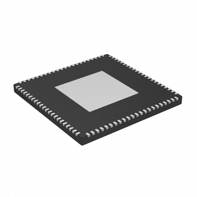
- Part No.:
- AD9915BCPZ
- Manufacturer:
- Analog Devices Inc.
- Category:
- Direct Digital Synthesis (DDS)
- Package:
- 88-VFQFN Exposed Pad, CSP
- Datasheet:
-
 AD9915BCPZ.pdf
- Description:
- IC DDS 2.5GHZ 12BIT 88LFCSP
- Quantity:
- Payment:

- Shipping:

Inventory:3,994
Please send an inquiry. Send us your inquiry, and we will respond immediately.
Product details
Overview
AD9915BCPZ from Analog Devices is a 2.5 GSPS direct digital synthesizer (DDS) with integrated 12-bit DAC, delivering frequency-agile sinusoidal outputs up to 1.0 GHz. It supports 135 pHz frequency tuning resolution, 16-bit phase tuning, and 12-bit amplitude scaling, enabling precise waveform synthesis for radar chirp generation and fast frequency-hopping communications.
For engineers reviewing the AD9915BCPZ datasheet, AD9915BCPZ pinout, AD9915BCPZ application, or AD9915BCPZ equivalent, key selection criteria include its 88-lead LFCSP package, multichip synchronization capability, PLL REF CLK multiplier, OSK modulation support, and dual-supply operation (1.8 V/3.3 V).
Technical Context
The AD9915BCPZ implements a high-speed DDS core synchronized to a 2.5 GHz system clock, with internal PLL multiplication of external reference inputs. Its 32-bit parallel datapath enables real-time polar modulation via direct FSK/PSK/ASK control through configurable function pins (F0–F3).
It integrates a calibrated 12-bit current-steering DAC with 50 Ω single-ended output impedance, programmable RSET-based full-scale current (20.48 mA), and on-chip reconstruction filtering. Multichip synchronization is achieved via dedicated SYNC_IN/SYNC_OUT pins and matched pipeline latency modes.
Key Specifications
| Parameter | Value and Actual Design Meaning |
|---|---|
| Max SYSCLK | 2.5 GSPS - Enables 1.0 GHz analog output in first Nyquist zone with 40% utilization margin. |
| DAC Resolution | 12-bit - Delivers 72 dB theoretical SNR and supports fine amplitude scaling (0–100% in 1/4096 steps). |
| Frequency Tuning | 135 pHz - Allows sub-mHz frequency step resolution at 1 GHz output using 64-bit tuning word in modulus mode. |
| Phase Noise | −128 dBc/Hz @ 1 kHz offset (978 MHz) - Meets stringent spectral purity requirements for LO synthesis in test equipment. |
| Wideband SFDR | < −57 dBc (typ. −60 dBc @ 978 MHz) - Specifies spurious-free dynamic range across full 0–1250 MHz output band. |
| Power Supplies | 1.8 V (core/DVDD) and 3.3 V (I/O/AVDD) - Dual-rail architecture isolates noise-sensitive analog DAC from digital logic domains. |
| Package | 88-lead LFCSP (12 mm × 12 mm × 0.85 mm) - Exposed pad improves thermal dissipation (θJA = 24.1°C/W) for sustained 2.8 W operation. |
Pinout & Package
AD9915BCPZ uses an 88-lead lead-frame chip-scale package (LFCSP) with exposed thermal pad soldered to PCB ground. The package supports high-density layout and efficient heat transfer in RF-intensive applications.
| Pin/Terminal | Circuit Role | Design Meaning |
|---|---|---|
| AOUT / AOUT | DAC complementary analog outputs | Single-ended 50 Ω-terminated voltage-mode outputs; require external AC coupling and balun for differential drive. |
| REF_CLK / REF_CLK | Differential reference clock input | AC-coupled 0.8–1.5 Vp-p input; supports bypassed or PLL-multiplied operation up to 2.5 GHz. |
| SYNC_CLK | Digital timing reference output | Provides synchronous edge for PS[2:0], I/O_UPDATE, and D[31:0] setup; critical for deterministic latency matching. |
| SYNC_IN / SYNC_OUT | Multi-chip synchronization interface | Enables phase-aligned operation across multiple AD9915BCPZ units; SYNC_OUT drives SYNC_IN of slave devices. |
| OSK | Output shift keying control | Direct amplitude gating pin; toggles DAC output between zero and programmed scale factor in manual or automatic sweep mode. |
| F0–F3 | Function configuration inputs | Selects serial/parallel interface mode and partitions D[31:0] for FSK/PSK/ASK modulation without register programming. |
Key Features
| Feature | Design Value |
|---|---|
| Programmable linear/nonlinear frequency sweeping | Configurable DRG (Digital Ramp Generator) with up/down control (DRCTL), hold (DRHOLD), and overflow flag (DROVER) for chirp generation. |
| 8 independent frequency/phase/amplitude profiles | Profile select pins PS0–PS2 enable hardware-triggered switching between preloaded tuning states with zero-latency update on SYNC_CLK edge. |
| Matched latency modes | Latency alignment across frequency/phase/amplitude updates ensures coherent multi-parameter modulation without timing skew. |
| Hardware-controlled power-down | EXT_PWR_DWN pin initiates full power-down (400–616 mW) with 45 ns entry and 250 ns exit time; preserves register state but loses DAC/PLL calibration. |
| Parallel + serial interface flexibility | 32-bit parallel port (D0–D31) or SPI-compatible serial port (SDIO/SCLK/CS) selectable via F0–F3; supports simultaneous read/write operations. |
Applications
| Agile LO Synthesis | FM Chirp Source |
|---|---|
|
Use Scenario: Rapidly reconfigurable local oscillator in S-band radar transceivers requiring microsecond-level frequency agility. IC Role / Device Role / Timing Role: Primary DDS signal source generating phase-coherent LO waveforms with sub-Hz tuning resolution and <1 µs hop time. Use Value: Eliminates need for VCO/PLL loop settling delays; enables true instantaneous frequency switching for pulse-Doppler processing. |
Use Scenario: Linear frequency-modulated (LFM) chirp generation for automotive radar front-ends operating at 77 GHz. IC Role / Device Role / Timing Role: Direct digital chirp generator using DRG-controlled frequency ramp with programmable start/stop points and slope. Use Value: Achieves monotonic, jitter-free sweeps without analog ramp circuitry; supports both rising and falling chirps via DRCTL pin. |
| Polar Modulator | Programmable Clock Generator |
|
Use Scenario: Baseband I/Q-to-RF polar modulation in software-defined radio transmitters with dynamic envelope tracking. IC Role / Device Role / Timing Role: DDS core modulates carrier phase/frequency while OSK pin controls amplitude scaling in real time. Use Value: Enables high-efficiency RF power amplifier operation by decoupling amplitude and phase paths with nanosecond-level coordination. |
Use Scenario: Low-jitter, multi-frequency clock source for FPGA-based test instrumentation requiring synchronized sampling clocks. IC Role / Device Role / Timing Role: Programmable clock synthesizer providing stable, digitally tunable outputs from DC to 1.0 GHz with <135 pHz step size. Use Value: Replaces multiple crystal oscillators and PLLs; simplifies BOM and eliminates board-level clock tree design complexity. |
Equivalent & Alternatives
The following parts are listed as comparable options for similar direct digital synthesizer applications.
| Alternative Part | Technical Difference | Application Difference | Selection Advice |
|---|---|---|---|
| AD9914BCPZ | Same 2.5 GSPS SYSCLK and 12-bit DAC, but lacks PLL REF CLK multiplier and has no DRG or OSK features. | Suitable only for fixed-reference clock systems without chirp or amplitude modulation needs. | Choose AD9914BCPZ when cost reduction is prioritized and PLL multiplication, sweep, or OSK are unnecessary. |
| AD9910BSVZ | 1 GSPS max SYSCLK, 14-bit DAC, wider 2.5 GHz output range (first Nyquist up to 500 MHz), no multichip sync pins. | Better SFDR at lower frequencies but lacks SYNC_IN/SYNC_OUT and matched latency modes for phased-array coherence. | Prefer AD9910BSVZ for ultra-high-resolution baseband synthesis where 14-bit amplitude fidelity outweighs 2.5 GSPS speed and synchronization. |
Compared with AD9915BCPZ, AD9914BCPZ omits critical radar and comms features like PLL multiplication and OSK, while AD9910BSVZ trades speed and synchronization capability for higher DAC resolution-making AD9915BCPZ uniquely suited for multichip, wideband, modulated RF synthesis.
Availability
AD9915BCPZ is available at Aetrix Electronics and suitable for agile LO synthesis, FM chirp generation, and programmable clocking applications requiring stable component supply, long-term lifecycle support, and traceable sourcing for aerospace and defense programs.
Supply support for AD9915BCPZ includes scheduled delivery planning, volume procurement assistance, BOM continuity management, traceable sourcing, and lifecycle availability coordination for OEM customers, industrial embedded developers, connected-device designers, and electronics production programs.
Manufacturer
Analog Devices is a global leader in high-performance analog, mixed-signal, and DSP technologies, serving precision instrumentation, communications, and industrial markets since 1965.
The AD9915BCPZ belongs to Analog Devices' high-speed DDS product line, engineered specifically for demanding RF signal generation in radar, electronic warfare, and automated test equipment where spectral purity, agility, and synchronization are critical.
FAQ
What is the maximum output frequency supported by the AD9915BCPZ?
The AD9915BCPZ supports analog output frequencies up to 1.0 GHz in the first Nyquist zone, limited by its 2.5 GSPS system clock (fOUT ≤ 0.4 × fSYSCLK). This is confirmed in the AC specifications table and functional description section of the Rev. G datasheet. The DAC output bandwidth and reconstruction filter design ensure usable signal integrity across this range, with measured SFDR performance validated up to 978.2 MHz.
Does the AD9915BCPZ require external reconstruction filtering?
Yes, the AD9915BCPZ requires external reconstruction filtering. While it includes internal current-source DAC architecture and RSET-based full-scale current control, the datasheet specifies that external passive LC or SAW filters must be used to suppress images and harmonics beyond the first Nyquist zone. Figure 21 and the "Reconstruction Filter" subsection confirm this requirement for clean analog output in RF applications.
How does multichip synchronization work on the AD9915BCPZ?
Multichip synchronization on the AD9915BCPZ is implemented via dedicated SYNC_IN and SYNC_OUT pins, along with matched pipeline latency modes. A master device drives SYNC_OUT (fSYSCLK/384) to SYNC_IN of slaves, aligning their internal clock domains. Register bit settings (CFR2[9]) and latency configuration ensure deterministic phase alignment across all synchronized AD9915BCPZ units, as detailed in the "Multiple Chip Synchronization" section.
Can the AD9915BCPZ operate without its internal PLL enabled?
Yes, the AD9915BCPZ can operate with the internal PLL disabled. The REF_CLK inputs accept 500–2500 MHz differential signals directly when the PLL is bypassed, as specified in Table 2 under "REF CLK Multiplier Bypassed." This mode reduces phase noise contribution from the PLL VCO but requires a low-jitter external clock source meeting the 0.8–1.5 Vp-p and 1 pF input capacitance requirements.
What is the purpose of the DAC_BP pin on the AD9915BCPZ?
The DAC_BP pin on the AD9915BCPZ provides access to the common control node of the DAC's current sources. Connecting a capacitor (typically 10–100 nF) between DAC_BP and AGND reduces high-frequency noise coupling into the DAC core, improving SFDR and phase noise performance-especially above 500 MHz. This is explicitly described in the Pin Function Descriptions table and verified in typical performance curves.
AD9915BCPZ Specifications
- Product attributes
- Attribute value
- Manufacturer:
- Analog Devices Inc.
- Series:
- -
- Package/Case:
- 88-VFQFN Exposed Pad, CSP
- Packaging:
- Tray
- Product Status:
- Active
- Resolution (Bits):
- 12 b
- Master fclk:
- 2.5 GHz
- Tuning Word Width (Bits):
- 32 b
- Voltage - Supply:
- 1.8V, 3.3V
- Operating Temperature:
- -40°C ~ 85°C
- Grade:
- -
- Qualification:
- -
- Mounting Type:
- Surface Mount
- Supplier Device Package:
- 88-LFCSP-VQ (12x12)
AD9915BCPZ FAQ
1.How can I place an order for AD9915BCPZ through Aetrix?
Please submit a Request for Quotation (RFQ) for AD9915BCPZ on Aetrix. Our sales agent will provide a competitive quotation and guide you through the order confirmation once you accept the terms.
2.Are the price and stock information for AD9915BCPZ reliable?
The price and inventory of AD9915BCPZ are updated periodically and may fluctuate due to market conditions. Stock and pricing data are typically refreshed every 24 hours. Quotation validity for AD9915BCPZ is usually 5 days.
3.What payment methods are accepted for AD9915BCPZ?
We accept Wire Transfer, PayPal, Credit Card, Western Union, MoneyGram, and Escrow for AD9915BCPZ transactions.
Note: Certain payment methods may incur a processing fee.
4.How is shipping managed for AD9915BCPZ?
AD9915BCPZ orders can be shipped via leading logistics carriers, including DHL, UPS, FedEx, TNT, or Registered Mail.
Once your AD9915BCPZ order is processed, you will receive an email with the shipment details and tracking number.
Note: Tracking information may take up to 24 hours to appear. Express delivery typically takes 3–5 business days.
5.How can I obtain technical support or documentation for AD9915BCPZ?
For technical support, including AD9915BCPZ datasheets, pinout diagrams, or application guidance, please contact our engineering support team. They can provide detailed documentation and assistance for your AD9915BCPZ requirements.
6.How does Aetrix verify that AD9915BCPZ is sourced from the original manufacturer or authorized distributors?
All AD9915BCPZ products on Aetrix are procured from qualified distributors and authorized channels. Our dedicated quality assurance team conducts strict verification, including traceability checks and, if necessary, third-party testing. This ensures that AD9915BCPZ meets industry standards.
7.What is the process for return or replacement of AD9915BCPZ?
All AD9915BCPZ units undergo pre-shipment inspection (PSI). If there is an issue with AD9915BCPZ, returns or replacements are accepted under the following conditions:
1.Quantity discrepancies, incorrect items, or visible external defects (such as breakage or corrosion), acknowledged by Aetrix.
2.The issue is reported within 90 days of delivery.
3.The AD9915BCPZ part is unused and in its original packaging.
Return procedure for AD9915BCPZ:
1.Submit a request within 90 days.
2.Obtain a Return Material Authorization (RMA) from Aetrix.
AD9915BCPZ Tags
-
AD9837ACPZ-RL
Analog Devices Inc.
-
AD9837ACPZ-RL7
Analog Devices Inc.
-
AD9837BCPZ-RL7
Analog Devices Inc.
-
AD9838BCPZ-RL7
Analog Devices Inc.
-
AD5932YRUZ
Analog Devices Inc.
-
AD9833BRMZ-REEL
Analog Devices Inc.
-
AD9833BRMZ-REEL7
Analog Devices Inc.
-
AD9833BRMZ
Analog Devices Inc.

-
AD9831ASTZ
Analog Devices Inc.
-
AD9834BRUZ-REEL7
Analog Devices Inc.
-
AD9834BRUZ
Analog Devices Inc.
-
AD9834CRUZ
Analog Devices Inc.
Tech Hub

A practical engineering guide to 3.3V and 5V logic compatibility, input thresholds, resistor dividers, translator ICs, MOSFET level shifting, I2C pull-ups, timing limits and power-sequencing risks.

The 74HC595 uses push-pull logic outputs, while the TPIC6B595 uses 50 V open-drain DMOS sinks for higher-power loads. This guide compares timing, current limits, 3.3 V interfacing, load wiring, thermal…

The 74HC595 converts serial data into eight stable parallel outputs. This guide covers pin functions, shift and storage timing, OE and MR behavior, drive-current limits, cascading, voltage compatibilit…

A technical comparison of level-sensitive latches and edge-triggered flip-flops, covering timing windows, setup and hold limits, master–slave operation, time borrowing, race-through, HDL inference and…

A D latch stores one bit while Enable controls when data can pass. This reference covers gate-level operation, truth tables, transparency, setup and hold timing, LE versus OE, common ICs and practical …

An SR latch stores one bit through cross-coupled feedback. This engineering reference covers NOR and NAND implementations, truth tables, forbidden-state recovery, gated operation, switch debouncing, fa…

Latch circuits retain one bit through feedback. This technical reference covers SR and D latches, truth tables, transparency, timing limits, latch-versus-flip-flop behavior, applications and common log…

An engineering guide to LED driver operation, constant-current and constant-voltage outputs, linear and switching topologies, dimming, IC selection, calculations, replacement compatibility, and fault c…

Operational amplifier guide covering op amp basics, feedback, ideal vs real op amps, common configurations, buffer circuits, offset, bias current, gain-bandwidth, slew rate, rail-to-rail limits and sel…

Jumper cables guide covering safe connection order, red and black clamp placement, final ground connection, cable gauge, length, clamp quality, copper vs CCA cables, jump starter comparison and battery…


