
 My Inquiry
 My Account


Analog Devices Inc. ADA4431-1YCPZ-R2
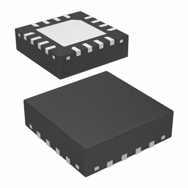
- Part No.:
- ADA4431-1YCPZ-R2
- Manufacturer:
- Analog Devices Inc.
- Category:
- Video Amps and Modules
- Package:
- 16-UFQFN Exposed Pad, CSP
- Datasheet:
-
 ADA4431-1YCPZ-R2.pdf
- Description:
- IC AMP FILTER 16LFCSP
- Quantity:
- Payment:

- Shipping:

Inventory:1,954
Please send an inquiry. Send us your inquiry, and we will respond immediately.
Product details
Overview
ADA4431-1YCPZ-R2 from Analog Devices is an ultralow-power SD video reconstruction filter with integrated load detection, third-order low-pass filtering (6 MHz 1 dB flatness), rail-to-rail output, and on-chip charge pump for dc-coupled video output. It operates from 2.5 V to 3.6 V, draws only 4.7 mA quiescent current in active mode, and supports portable video applications requiring automatic power-down when no video load is present.
For engineers reviewing the ADA4431-1YCPZ-R2 datasheet, ADA4431-1YCPZ-R2 pinout, ADA4431-1YCPZ-R2 application, or ADA4431-1YCPZ-R2 equivalent, key selection considerations include load-detect autonomy, SAG correction capability for ac-coupled outputs, −3 dB bandwidth (6.6–9.1 MHz), differential gain (0.7%), and 16-lead 3 mm × 3 mm LFCSP package compatibility with space-constrained handheld designs.
Technical Context
The ADA4431-1YCPZ-R2 integrates a third-order video low-pass filter with programmable gain (G = 2 or G ≈ 2.5 with SAG), a charge pump generating a virtual negative supply for true dc-coupled output (sync tip at −300 mV), and autonomous load detection using FB1/FB2 feedback pins across a 75 Ω termination resistor. Its disable pin (DIS) controls three states: high (charge pump enabled), floating (charge pump disabled), and low (full shutdown).
It features rail-to-rail output driving capability (40 mA linear current), input-to-output isolation of 89 dB at 1 MHz in disabled state, and dual operating modes: charge pump on (output range −0.8 V to +2.8 V) or off (0 V to +2.8 V). SAG correction reduces required ac-coupling capacitor size by enabling low-frequency gain boost while maintaining flat passband response.
Key Specifications
| Parameter | Value and Actual Design Meaning |
|---|---|
| −3 dB Bandwidth | 6.6–9.1 MHz (ensures full NTSC/PAL baseband signal integrity without aliasing) |
| 1 dB Flatness | 6 MHz (maintains luminance fidelity across standard-definition video bandwidth) |
| Quiescent Supply Current | 4.7 mA typical (enables >10-hour battery life in portable media players) |
| Differential Gain / Phase | 0.7% / 0.3° (meets ITU-R BT.470-6 color fidelity requirements) |
| Output Voltage Range | −0.8 V to +2.8 V (supports dc-coupled sync-tip-to-black-level alignment) |
| Load Detection Threshold | Autonomous detection of 75 Ω video load via FB1/FB2 (eliminates need for external controller polling) |
| Package | 16-lead LFCSP_UQ, 3 mm × 3 mm × 0.55 mm (fits 0.5 mm pitch PCB layouts in ultra-thin devices) |
Pinout & Package
ADA4431-1YCPZ-R2 is housed in a 16-lead Lead Frame Chip Scale Package (LFCSP_UQ), CP-16-12, with exposed pad thermally connected to PCB ground plane. Package dimensions: 3.00 mm × 3.00 mm body, 0.55 mm max height, JEDEC MO-248-UEED compliant.
| Pin/Terminal | Circuit Role | Design Meaning |
|---|---|---|
| 1, 10, +VS | Positive Supply Input | Dual supply pins reduce IR drop; accepts 2.5 V–3.6 V single supply |
| 2, IN | Video Signal Input | High-impedance (10 MΩ), low-capacitance (1 pF) input compatible with DAC/encoder outputs |
| 3, DIS | Disable Control Input | Three-state logic: high = charge pump on; floating = charge pump off; low = full shutdown (24 µA) |
| 4, LDO | Load Detect Output | Open-drain logic output indicating video load presence (high = 75 Ω detected) |
| 5–6, CAP4/CAP3 | Charge Pump Capacitor Terminals | Connect external 0.1 µF ceramic caps to generate virtual negative rail |
| 7, 12, GND | Ground Reference | Multiple ground pins minimize ground bounce in high-speed video paths |
| 8–9, CAP2/CAP1 | SAG Correction Capacitor Terminals | Enable frequency-dependent gain boost for smaller ac-coupling capacitors |
| 11, SUBS | Substrate Bias | Bypass to GND with 1.0 µF capacitor to stabilize internal reference |
| 13, SAG | SAG Feedback Input | Connects to output to enable low-frequency gain compensation |
| 14, OUT | Filtered Video Output | Rail-to-rail buffer drives two 75 Ω terminated loads simultaneously |
| 15–16, FB2/FB1 | Load Detect Feedback | Monitor voltage drop across external 75 Ω series termination to detect load presence |
Key Features
| Feature | Design Value |
|---|---|
| Integrated Load Detection | Autonomous monitoring of 75 Ω video load via FB1/FB2; powers down to 0.1 mA when disconnected |
| On-Chip Charge Pump | Generates virtual negative supply from single 2.5 V–3.6 V rail, enabling true dc-coupled output with −300 mV sync tip |
| SAG Correction | Compensates for RC droop in ac-coupled outputs, allowing use of 22 µF/47 µF instead of ≥220 µF capacitors |
| Rail-to-Rail Output Driver | Delivers 40 mA linear current into dual 75 Ω loads while maintaining 0.7% differential gain and 0.3° phase error |
| Low-Power Disable States | Three operational modes: active (4.7 mA), load-search (0.1 mA), and disabled (24 µA) - all controlled by DIS pin voltage |
Applications
| Portable Media Players | Cell Phones |
|---|---|
Use Scenario: Driving composite video output to external monitors or TVs via 3.5 mm AV jack. IC Role / Device Role / Timing Role: SD video reconstruction filter and load-aware driver with automatic power-down when cable is unplugged. Use Value: Extends battery life by reducing system power draw by >97% during idle video output periods. |
Use Scenario: Feeding baseband video signal from application processor to analog video encoder before HDMI or CVBS output. IC Role / Device Role / Timing Role: Final-stage filter and buffer ensuring compliance with NTSC/PAL spectral mask and timing jitter limits. Use Value: Eliminates need for discrete op-amp + external charge pump, saving 32 mm² PCB area and BOM cost. |
| Digital Still Cameras | Portable DVD Players |
Use Scenario: Transmitting live viewfinder or playback video over mini-B AV port to external display. IC Role / Device Role / Timing Role: Low-noise, low-distortion video driver with SAG correction for compact ac-coupled output stage. Use Value: Enables use of 47 µF/22 µF ceramic capacitors instead of bulky 220 µF tantalum, reducing height and improving reliability. |
Use Scenario: Delivering decoded SD video to composite output connector with automatic load sensing. IC Role / Device Role / Timing Role: Integrated filter, driver, and load detector replacing discrete filter + buffer + comparator solution. Use Value: Reduces component count by 7 parts and eliminates manual calibration of load-detect threshold resistors. |
Equivalent & Alternatives
The following parts are listed as comparable options for similar SD video filter applications.
| Alternative Part | Technical Difference | Application Difference | Selection Advice |
|---|---|---|---|
| MAX4392ESE+ | No integrated load detection or charge pump; requires external negative supply for dc-coupled output. | Lacks autonomous power management; unsuitable for battery-powered devices needing load-aware shutdown. | Select MAX4392ESE+ only if system already provides dual supplies and load detection is handled externally. |
| LMH0394SQ/NOPB | Designed for HD-SDI (1.485 Gbps); not optimized for SD baseband filtering; higher quiescent current (18 mA). | Over-specified for SD video; incompatible pinout and bandwidth; no SAG correction or load detection. | LMH0394SQ/NOPB is not functionally interchangeable; use only in HD video infrastructure, not portable SD applications. |
Compared with MAX4392ESE+ and LMH0394SQ/NOPB, the ADA4431-1YCPZ-R2 uniquely combines ultralow power (4.7 mA), integrated load detection, and on-chip charge pump in a 3 mm × 3 mm package-making it the only viable option for space- and battery-constrained portable SD video systems requiring zero-external-component dc coupling.
Availability
ADA4431-1YCPZ-R2 is available at Aetrix Electronics and suitable for portable media players, cell phones, and digital still cameras requiring stable component supply, long-term lifecycle support, and RoHS-compliant packaging.
Supply support for ADA4431-1YCPZ-R2 includes scheduled delivery planning, volume procurement assistance, BOM continuity management, traceable sourcing, and lifecycle availability coordination for OEM customers, industrial embedded developers, connected-device designers, and electronics production programs.
Manufacturer
Analog Devices, Inc. is a global leader in high-performance analog, mixed-signal, and digital signal processing semiconductors, headquartered in Norwood, MA, serving industrial, automotive, communications, and consumer markets.
The ADA4431-1YCPZ-R2 belongs to Analog Devices' portable video interface product line, engineered specifically for ultralow-power SD video signal conditioning in battery-operated handheld devices with strict size and thermal constraints.
FAQ
What is the primary function of the ADA4431-1YCPZ-R2 in a video signal chain?
The ADA4431-1YCPZ-R2 serves as a fully integrated SD video reconstruction filter and driver. It performs third-order low-pass filtering (6 MHz 1 dB flatness), provides rail-to-rail buffered output capable of driving dual 75 Ω loads, implements autonomous load detection to reduce power when no video load is present, and incorporates an on-chip charge pump for dc-coupled output. This makes ADA4431-1YCPZ-R2 ideal for portable devices where power, size, and signal fidelity are critical.
How does the load detection feature of the ADA4431-1YCPZ-R2 operate without external components?
The ADA4431-1YCPZ-R2 uses its FB1 and FB2 pins to monitor voltage drop across an external 75 Ω series termination resistor placed between the OUT pin and the video load. When a 75 Ω load is connected, current flow creates a measurable voltage difference that the internal circuitry detects autonomously. The LDO pin then asserts high to indicate load presence. No microcontroller polling or external comparators are needed - ADA4431-1YCPZ-R2 manages this entirely internally.
Can the ADA4431-1YCPZ-R2 be used with ac-coupled video outputs, and what advantage does SAG correction provide?
Yes, the ADA4431-1YCPZ-R2 supports both dc-coupled (with charge pump enabled) and ac-coupled outputs (with charge pump disabled). When used ac-coupled, its SAG correction feature compensates for low-frequency droop caused by series coupling capacitors. By connecting external capacitors to CAP1–CAP4 and routing SAG to OUT, ADA4431-1YCPZ-R2 boosts low-frequency gain, allowing use of smaller 22 µF/47 µF ceramics instead of bulky 220 µF electrolytics - reducing board area and improving reliability.
What are the supply voltage requirements and power consumption modes of the ADA4431-1YCPZ-R2?
The ADA4431-1YCPZ-R2 operates from a single 2.5 V to 3.6 V supply. It offers three distinct power modes: normal active mode (4.7 mA typical with load present and charge pump on), load-search mode (0.1 mA when no load is detected but monitoring continues), and disabled mode (24 µA when DIS pin is pulled low). These modes are controlled solely by the DIS pin voltage level - high, floating, or low - enabling flexible system-level power management without firmware intervention.
Is the ADA4431-1YCPZ-R2 pin-compatible with other members of the ADA4431 family, such as the ADA4431-0?
No, the ADA4431-1YCPZ-R2 is not pin-compatible with the ADA4431-0. While both share the same 16-lead LFCSP package and core architecture, the ADA4431-0 lacks load detection, SAG correction, and the LDO/FB1/FB2 pins. Pin functions differ significantly - for example, pins 4 (LDO), 13 (SAG), 15 (FB2), and 16 (FB1) are unique to ADA4431-1YCPZ-R2 and have no counterpart on ADA4431-0. PCB layout and firmware must be redesigned to migrate from ADA4431-0 to ADA4431-1YCPZ-R2.
ADA4431-1YCPZ-R2 Specifications
- Product attributes
- Attribute value
- Manufacturer:
- Analog Devices Inc.
- Package/Case:
- 16-UFQFN Exposed Pad, CSP
- Series:
- -
- Packaging:
- Tape & Reel (TR)
- Product Status:
- Discontinued at Digi-Key
- Applications:
- Filter
- Output Type:
- Rail-to-Rail
- Number of Circuits:
- 1
- -3db Bandwidth:
- 7.9 MHz
- Slew Rate:
- -
- Current - Supply:
- 4.7 mA
- Current - Output / Channel:
- -
- Voltage - Supply, Single/Dual (±):
- 2.5V ~ 3.6V
- Mounting Type:
- Surface Mount
- Grade:
- -
- Qualification:
- -
- Supplier Device Package:
- 16-LFCSP-UQ (3x3)
ADA4431-1YCPZ-R2 FAQ
1.How can I place an order for ADA4431-1YCPZ-R2 through Aetrix?
Please submit a Request for Quotation (RFQ) for ADA4431-1YCPZ-R2 on Aetrix. Our sales agent will provide a competitive quotation and guide you through the order confirmation once you accept the terms.
2.Are the price and stock information for ADA4431-1YCPZ-R2 reliable?
The price and inventory of ADA4431-1YCPZ-R2 are updated periodically and may fluctuate due to market conditions. Stock and pricing data are typically refreshed every 24 hours. Quotation validity for ADA4431-1YCPZ-R2 is usually 5 days.
3.What payment methods are accepted for ADA4431-1YCPZ-R2?
We accept Wire Transfer, PayPal, Credit Card, Western Union, MoneyGram, and Escrow for ADA4431-1YCPZ-R2 transactions.
Note: Certain payment methods may incur a processing fee.
4.How is shipping managed for ADA4431-1YCPZ-R2?
ADA4431-1YCPZ-R2 orders can be shipped via leading logistics carriers, including DHL, UPS, FedEx, TNT, or Registered Mail.
Once your ADA4431-1YCPZ-R2 order is processed, you will receive an email with the shipment details and tracking number.
Note: Tracking information may take up to 24 hours to appear. Express delivery typically takes 3–5 business days.
5.How can I obtain technical support or documentation for ADA4431-1YCPZ-R2?
For technical support, including ADA4431-1YCPZ-R2 datasheets, pinout diagrams, or application guidance, please contact our engineering support team. They can provide detailed documentation and assistance for your ADA4431-1YCPZ-R2 requirements.
6.How does Aetrix verify that ADA4431-1YCPZ-R2 is sourced from the original manufacturer or authorized distributors?
All ADA4431-1YCPZ-R2 products on Aetrix are procured from qualified distributors and authorized channels. Our dedicated quality assurance team conducts strict verification, including traceability checks and, if necessary, third-party testing. This ensures that ADA4431-1YCPZ-R2 meets industry standards.
7.What is the process for return or replacement of ADA4431-1YCPZ-R2?
All ADA4431-1YCPZ-R2 units undergo pre-shipment inspection (PSI). If there is an issue with ADA4431-1YCPZ-R2, returns or replacements are accepted under the following conditions:
1.Quantity discrepancies, incorrect items, or visible external defects (such as breakage or corrosion), acknowledged by Aetrix.
2.The issue is reported within 90 days of delivery.
3.The ADA4431-1YCPZ-R2 part is unused and in its original packaging.
Return procedure for ADA4431-1YCPZ-R2:
1.Submit a request within 90 days.
2.Obtain a Return Material Authorization (RMA) from Aetrix.
ADA4431-1YCPZ-R2 Tags

-
LT6552CS8#PBF
Analog Devices Inc.
-
LT6205IS5#TRPBF
Analog Devices Inc.
-
LT6206IMS8#TRPBF
Analog Devices Inc.
-
LT6552CDD#PBF
Analog Devices Inc.
-
LT6552IS8#PBF
Analog Devices Inc.
-
LT1252CS8#PBF
Analog Devices Inc.
-
AD818ARZ-REEL7
Analog Devices Inc.

-
MAX4310EUA+
Analog Devices Inc./Maxim Integrated
-
AD829ARZ
Analog Devices Inc.
-
AD810ARZ
Analog Devices Inc.

-
MAX4310ESA+
Analog Devices Inc./Maxim Integrated
-
MAX4313ESA+
Analog Devices Inc./Maxim Integrated
Tech Hub

A practical engineering guide to 3.3V and 5V logic compatibility, input thresholds, resistor dividers, translator ICs, MOSFET level shifting, I2C pull-ups, timing limits and power-sequencing risks.

The 74HC595 uses push-pull logic outputs, while the TPIC6B595 uses 50 V open-drain DMOS sinks for higher-power loads. This guide compares timing, current limits, 3.3 V interfacing, load wiring, thermal…

The 74HC595 converts serial data into eight stable parallel outputs. This guide covers pin functions, shift and storage timing, OE and MR behavior, drive-current limits, cascading, voltage compatibilit…

A technical comparison of level-sensitive latches and edge-triggered flip-flops, covering timing windows, setup and hold limits, master–slave operation, time borrowing, race-through, HDL inference and…

A D latch stores one bit while Enable controls when data can pass. This reference covers gate-level operation, truth tables, transparency, setup and hold timing, LE versus OE, common ICs and practical …

An SR latch stores one bit through cross-coupled feedback. This engineering reference covers NOR and NAND implementations, truth tables, forbidden-state recovery, gated operation, switch debouncing, fa…

Latch circuits retain one bit through feedback. This technical reference covers SR and D latches, truth tables, transparency, timing limits, latch-versus-flip-flop behavior, applications and common log…

An engineering guide to LED driver operation, constant-current and constant-voltage outputs, linear and switching topologies, dimming, IC selection, calculations, replacement compatibility, and fault c…

Operational amplifier guide covering op amp basics, feedback, ideal vs real op amps, common configurations, buffer circuits, offset, bias current, gain-bandwidth, slew rate, rail-to-rail limits and sel…

Jumper cables guide covering safe connection order, red and black clamp placement, final ground connection, cable gauge, length, clamp quality, copper vs CCA cables, jump starter comparison and battery…


