
 My Inquiry
 My Account


Analog Devices Inc. ADATE207BBPZ
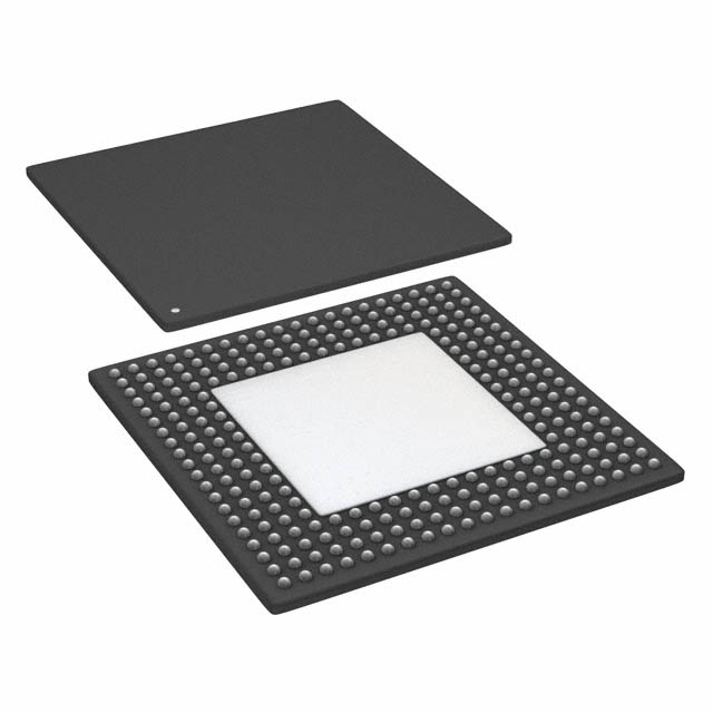
- Part No.:
- ADATE207BBPZ
- Manufacturer:
- Analog Devices Inc.
- Category:
- Application Specific Clock/Timing
- Package:
- 256-LBGA Exposed Pad
- Datasheet:
-
 ADATE207BBPZ.pdf
- Description:
- IC TIMING FORMATTER QUAD 256BGA
- Quantity:
- Payment:

- Shipping:

Inventory:1,875
Please send an inquiry. Send us your inquiry, and we will respond immediately.
Product details
Overview
ADATE207BBPZ from Analog Devices is a quad-channel timing formatter IC for automatic test equipment (ATE), delivering 100 MHz base vector rate, 39.06 ps edge placement resolution, 2.5 ns minimum edge refire rate, and STIL IEEE 1450-1999-compatible event generation per channel. It interfaces between pattern memory and DCL chips to drive, compare, and capture digital pin responses in high-speed ATE systems.
For engineers reviewing the ADATE207BBPZ datasheet, ADATE207BBPZ pinout, ADATE207BBPZ application, or ADATE207BBPZ equivalent, this device supports ×2/×4 high-speed modes, differential DCL interface control, 4-bit DUT capture per channel, and TMU multiplexer support for time measurement unit integration in production-grade ATE platforms.
Technical Context
The ADATE207BBPZ implements four independent timing channels, each with 256 programmable waveforms and four STIL-compatible events per waveform. Each event uses a dual-stage delay generator combining 16-bit integer counts of 2.5 ns clock cycles and a 6-bit analog vernier for 39.06 ps resolution.
It features differential DCL interface logic with open-drain drive/compare outputs, 4-bit per-channel DUT capture, 32-bit fail accumulation registers, and three 8-to-1 TMU multiplexers supporting arm/start/stop signal routing. The device operates from a single 2.5 V supply and integrates low-jitter clock input multiplexing onto Channel 2/3 DR_DATA pins.
Key Specifications
| Parameter | Value and Actual Design Meaning |
|---|---|
| Base Vector Rate | 100 MHz - defines maximum pattern burst throughput and system timing granularity. |
| Edge Placement Resolution | 39.06 ps - enables sub-ns precision in edge positioning for high-fidelity waveform synthesis. |
| Min Edge Refire Rate | 2.5 ns - supports ultra-fast sequential edge generation without timing violation. |
| Waveforms per Channel | 256 - allows complex test pattern sequencing with minimal external memory overhead. |
| Fail Accumulation Register | 32-bit per channel - provides robust failure logging for statistical yield analysis in production ATE. |
| DUT Capture Width | 4-bit per channel - enables mixed-signal receive memory applications with compact data path. |
| Power Dissipation | 6.3–7.1 W at full load - optimized for air-cooled ATE card-level thermal management. |
| Supply Voltage | 2.5 V ±5% - matches industry-standard LVCMOS25 I/O voltage for seamless integration with ATE controller ASICs. |
Pinout & Package
ADATE207BBPZ is housed in a 256-ball BGA_ED package (27 mm × 27 mm body, 1.27 mm pitch) with thermally enhanced construction (θJA = 14.3°C/W in still air). Ball grid includes dedicated power/ground planes (VDD/VSS/IOVDD/IOVSS), differential DCL I/O pairs, LVCMOS25 control/data buses, and analog thermal sensing (T_DIODE) and current reference (REF_1K) terminals.
| Pin/Terminal | Circuit Role | Design Meaning |
|---|---|---|
| DR_DATA_CH0_P/N to CH3_P/N | Differential drive data outputs | Open-drain LVDS-compatible signals driving DCL chip inputs; support ×2 pin multiplexing. |
| COMP_H_CHx_P/N & COMP_L_CHx_P/N | Differential comparator inputs | Terminated 50 Ω differential inputs comparing DUT output against VOH/VOL thresholds. |
| PAT_DUTDATA_x[3:0] | DUT response capture outputs | LVCMOS25 4-bit parallel capture of DUT logic states per channel for pass/fail analysis. |
| CS_AD[15:0], CS_AS, CS_RW_B | Bidirectional CSR interface | Multiplexed address/data bus for real-time register read/write access during pattern execution. |
| TMU_ARM_P/N, START_P/N, STOP_P/N | TMU multiplexer outputs | Three independent differential tristate outputs routing comparator results to external time measurement units. |
Key Features
| Feature | Design Value |
|---|---|
| STIL IEEE 1450-1999 compatibility | Enables direct integration with industry-standard ATE pattern compilers and test program generators. |
| ×2 and ×4 high-speed modes | Allows doubling or quadrupling effective vector rate without increasing master clock frequency. |
| Programmable global INPUT_DELAY[7:0] | Applies uniform timing offset across all 16 edges (4 per channel), simplifying system-level skew calibration. |
| Differential DCL interface control | Reduces EMI and improves noise immunity in dense ATE backplane environments. |
| On-chip temperature diode (T_DIODE) | Enables real-time die temperature monitoring for thermal derating and reliability validation. |
| 4-period edge span with vernier delay | Supports flexible timing windows up to 163.8 μs while maintaining 39.06 ps resolution within each period. |
Applications
| ATE Digital Pin Conditioning | High-Speed Pulse Generation |
|---|---|
Use Scenario: Generating precise stimulus waveforms and validating DUT responses in semiconductor final test handlers. IC Role / Device Role / Timing Role: Quad-channel timing formatter synchronizing drive, compare, and capture operations across four digital pins per device under test. Use Value: Enables 100 MHz vector rates with 39.06 ps edge placement accuracy, directly supporting advanced process node test requirements. | Use Scenario: Creating calibrated multi-edge pulse trains for jitter tolerance testing of SerDes receivers. IC Role / Device Role / Timing Role: Programmable edge generator producing up to four independent events per waveform with sub-ns retrigger capability. Use Value: Delivers 2.5 ns minimum refire rate and 1 ns minimum pulse width, meeting stringent pulse fidelity demands in compliance test fixtures. |
| Time Measurement Unit Interface | Mixed-Signal Test Instrumentation |
Use Scenario: Routing comparator outputs to external TMUs for precise timing parameter extraction (e.g., setup/hold, propagation delay). IC Role / Device Role / Timing Role: TMU multiplexer hub providing three 8-to-1 differential outputs (ARM/START/STOP) from any channel's dual comparators. Use Value: Eliminates external multiplexer ICs and reduces signal path skew, improving measurement repeatability in metrology-grade instruments. | Use Scenario: Capturing analog-digital boundary behavior in mixed-signal SoCs using digital pin capture synchronized to analog stimulus. IC Role / Device Role / Timing Role: 4-bit per-channel DUT data capture engine with MCLK-synchronized sampling and fail flagging. Use Value: Provides deterministic 4-bit response capture aligned to timing edges, enabling correlation of analog anomalies with digital state transitions. |
Equivalent & Alternatives
The following parts are listed as comparable options for similar timing formatter applications.
| Alternative Part | Technical Difference | Application Difference | Selection Advice |
|---|---|---|---|
| ADATE305BBCZ | 8-channel architecture, 200 MHz base rate, 19.53 ps resolution, integrated PLL clock generator | Higher channel count and resolution suited for next-gen ATE with increased pin density | Select when scaling beyond 4-channel capacity or requiring on-chip clock multiplication |
| ADATE212BBPZ | Same 4-channel architecture but adds JESD204B serializer interface and enhanced fail reporting registers | Optimized for ATE systems integrating FPGA-based pattern generators via high-speed serial links | Select when replacing legacy parallel CSR interface with JESD204B for reduced interconnect complexity |
Compared with ADATE207BBPZ, ADATE305BBCZ offers double the channel count and finer timing resolution at higher power, while ADATE212BBPZ retains identical timing performance but replaces parallel CSR with JESD204B-making it preferable for FPGA-hosted ATE architectures requiring serial configuration bandwidth.
Availability
ADATE207BBPZ is available at Aetrix Electronics and suitable for automatic test equipment (ATE), high-speed digital instrumentation, pulse generation systems, and time measurement unit interfaces requiring stable component supply and long-term lifecycle support.
Supply support for ADATE207BBPZ includes scheduled delivery planning, volume procurement assistance, BOM continuity management, traceable sourcing, and lifecycle availability coordination for OEM customers, industrial embedded developers, connected-device designers, and electronics production programs.
Manufacturer
Analog Devices, Inc. is a global leader in high-performance analog, mixed-signal, and digital signal processing semiconductors, headquartered in Norwood, MA.
The ADATE product line delivers precision timing generators and formatters specifically engineered for automatic test equipment, emphasizing sub-ns edge resolution, STIL compliance, and robust DCL interface integration.
FAQ
What is the primary function of the ADATE207BBPZ in an ATE system?
The ADATE207BBPZ serves as a quad-channel timing formatter that bridges pattern memory and DCL (driver/comparator/load) chips. It generates precisely timed drive signals, performs real-time DUT response comparison against expected levels, and captures 4-bit DUT data per channel-all synchronized to a 100 MHz base vector rate. Its role in the ADATE207BBPZ-based ATE architecture is to ensure nanosecond-accurate stimulus application and response evaluation across four digital pins simultaneously.
Does the ADATE207BBPZ support STIL-compliant waveform definition?
Yes, the ADATE207BBPZ natively supports STIL IEEE 1450-1999-compatible events including drive high/low, force up/down, compare high/low/window, and unknown/valid states. Each of its 256 waveforms per channel can contain up to four such events, with programmable timing edges mapped directly to STIL event codes. This ensures seamless interoperability with industry-standard ATE pattern compilers and test program generators used with the ADATE207BBPZ.
How does the ADATE207BBPZ achieve 39.06 ps timing resolution?
The ADATE207BBPZ achieves 39.06 ps resolution through a hybrid delay architecture: a 16-bit integer counter operating at 2.5 ns steps (400 MHz equivalent) combined with a 6-bit analog vernier that subdivides each 2.5 ns interval into 64 equal parts (2.5 ns ÷ 64 = 39.06 ps). This vernier uses a compensated CMOS timing cell calibrated across process/voltage/temperature, and the total delay is the sum of waveform memory delay, per-event calibration offset, and global 8-bit INPUT_DELAY value-all applied per edge in the ADATE207BBPZ.
Can the ADATE207BBPZ interface with external time measurement units (TMUs)?
Yes, the ADATE207BBPZ integrates a dedicated TMU multiplexer with three 8-to-1 differential outputs: TMU_ARM_P/N, TMU_START_P/N, and TMU_STOP_P/N. These outputs route comparator results (high/low compare flags) from any of the four channels' dual comparators to external TMUs. This eliminates need for discrete multiplexers and preserves signal integrity-enabling precise timing parameter extraction like propagation delay or setup/hold time in ADATE207BBPZ-based ATE systems.
What power supply requirements does the ADATE207BBPZ have?
The ADATE207BBPZ requires a single 2.5 V ±5% supply (2.375 V to 2.625 V) for core logic and I/O operation. Power dissipation ranges from 5.7 W (idle) to 7.1 W (full-load pattern bursting at 100 MHz). It uses separate IOVDD/IOVSS planes for I/O circuitry and includes explicit decoupling guidance: eight 0.1 μF ceramic capacitors placed near the 256-ball BGA_ED package corners and mid-sides, plus 10 μF tantalum/ceramic bulk capacitance around the perimeter. This power architecture ensures stable operation of the ADATE207BBPZ in thermally constrained ATE card slots.
ADATE207BBPZ Specifications
- Product attributes
- Attribute value
- Manufacturer:
- Analog Devices Inc.
- Series:
- -
- Package/Case:
- 256-LBGA Exposed Pad
- Packaging:
- Tray
- Product Status:
- Obsolete
- Programmable:
- Not Verified
- PLL:
- Yes
- Main Purpose:
- Automatic Test Equipment
- Input:
- -
- Output:
- -
- Number of Circuits:
- 4
- Ratio - Input:Output:
- -
- Differential - Input:Output:
- -
- Frequency - Max:
- 100MHz
- Voltage - Supply:
- 2.375V ~ 2.625V
- Operating Temperature:
- -25°C ~ 85°C
- Mounting Type:
- Surface Mount
- Grade:
- -
- Qualification:
- -
- Supplier Device Package:
- 256-BGA-ED (27x27)
ADATE207BBPZ FAQ
1.How can I place an order for ADATE207BBPZ through Aetrix?
Please submit a Request for Quotation (RFQ) for ADATE207BBPZ on Aetrix. Our sales agent will provide a competitive quotation and guide you through the order confirmation once you accept the terms.
2.Are the price and stock information for ADATE207BBPZ reliable?
The price and inventory of ADATE207BBPZ are updated periodically and may fluctuate due to market conditions. Stock and pricing data are typically refreshed every 24 hours. Quotation validity for ADATE207BBPZ is usually 5 days.
3.What payment methods are accepted for ADATE207BBPZ?
We accept Wire Transfer, PayPal, Credit Card, Western Union, MoneyGram, and Escrow for ADATE207BBPZ transactions.
Note: Certain payment methods may incur a processing fee.
4.How is shipping managed for ADATE207BBPZ?
ADATE207BBPZ orders can be shipped via leading logistics carriers, including DHL, UPS, FedEx, TNT, or Registered Mail.
Once your ADATE207BBPZ order is processed, you will receive an email with the shipment details and tracking number.
Note: Tracking information may take up to 24 hours to appear. Express delivery typically takes 3–5 business days.
5.How can I obtain technical support or documentation for ADATE207BBPZ?
For technical support, including ADATE207BBPZ datasheets, pinout diagrams, or application guidance, please contact our engineering support team. They can provide detailed documentation and assistance for your ADATE207BBPZ requirements.
6.How does Aetrix verify that ADATE207BBPZ is sourced from the original manufacturer or authorized distributors?
All ADATE207BBPZ products on Aetrix are procured from qualified distributors and authorized channels. Our dedicated quality assurance team conducts strict verification, including traceability checks and, if necessary, third-party testing. This ensures that ADATE207BBPZ meets industry standards.
7.What is the process for return or replacement of ADATE207BBPZ?
All ADATE207BBPZ units undergo pre-shipment inspection (PSI). If there is an issue with ADATE207BBPZ, returns or replacements are accepted under the following conditions:
1.Quantity discrepancies, incorrect items, or visible external defects (such as breakage or corrosion), acknowledged by Aetrix.
2.The issue is reported within 90 days of delivery.
3.The ADATE207BBPZ part is unused and in its original packaging.
Return procedure for ADATE207BBPZ:
1.Submit a request within 90 days.
2.Obtain a Return Material Authorization (RMA) from Aetrix.
ADATE207BBPZ Tags
-
LMK00334RTVRQ1
Texas Instruments
.jpg)
-
DSC557-0344FI0T
Microchip Technology
-
9FGV0241AKILFT
Renesas

-
9DBL0452CKILFT
Renesas
-
DSC557-0344FL1T
Microchip Technology
-
RC19008AGND#KB0
Renesas
-
RC19008AGND#BB0
Renesas

-
9DB403DGILFT
Renesas
-
9DB233AGILFT
Renesas

-
9DB803DGILFT
Renesas
-
9FGL0851DKILFT
Renesas
-
AB-557-03-HCHC-F-L-C-T
Abracon LLC
Tech Hub

A practical engineering guide to 3.3V and 5V logic compatibility, input thresholds, resistor dividers, translator ICs, MOSFET level shifting, I2C pull-ups, timing limits and power-sequencing risks.

The 74HC595 uses push-pull logic outputs, while the TPIC6B595 uses 50 V open-drain DMOS sinks for higher-power loads. This guide compares timing, current limits, 3.3 V interfacing, load wiring, thermal…

The 74HC595 converts serial data into eight stable parallel outputs. This guide covers pin functions, shift and storage timing, OE and MR behavior, drive-current limits, cascading, voltage compatibilit…

A technical comparison of level-sensitive latches and edge-triggered flip-flops, covering timing windows, setup and hold limits, master–slave operation, time borrowing, race-through, HDL inference and…

A D latch stores one bit while Enable controls when data can pass. This reference covers gate-level operation, truth tables, transparency, setup and hold timing, LE versus OE, common ICs and practical …

An SR latch stores one bit through cross-coupled feedback. This engineering reference covers NOR and NAND implementations, truth tables, forbidden-state recovery, gated operation, switch debouncing, fa…

Latch circuits retain one bit through feedback. This technical reference covers SR and D latches, truth tables, transparency, timing limits, latch-versus-flip-flop behavior, applications and common log…

An engineering guide to LED driver operation, constant-current and constant-voltage outputs, linear and switching topologies, dimming, IC selection, calculations, replacement compatibility, and fault c…

Operational amplifier guide covering op amp basics, feedback, ideal vs real op amps, common configurations, buffer circuits, offset, bias current, gain-bandwidth, slew rate, rail-to-rail limits and sel…

Jumper cables guide covering safe connection order, red and black clamp placement, final ground connection, cable gauge, length, clamp quality, copper vs CCA cables, jump starter comparison and battery…


