
 My Inquiry
 My Account


Texas Instruments ADC081S021EVAL

- Part No.:
- ADC081S021EVAL
- Manufacturer:
- Texas Instruments
- Package:
- Datasheet:
-
 ADC081S021EVAL.pdf
- Description:
- BOARD EVALUATION FOR ADC081S021
- Quantity:
- Payment:

- Shipping:

Inventory:2,104
Please send an inquiry. Send us your inquiry, and we will respond immediately.
Product details
Overview
ADC081S021EVAL from Texas Instruments is an evaluation board for the ADC081S021, a single-channel, 8-bit successive-approximation analog-to-digital converter (SAR ADC) operating at 50–200 ksps with SPI-compatible serial interface. It supports 2.7–5.25 V supply, delivers 49.6 dB SNR (typ), and features power-down mode reducing consumption to 2.6 µW. Designed for rapid prototyping of low-power sensor signal chains in portable instrumentation.
For engineers reviewing the ADC081S021EVAL datasheet, ADC081S021EVAL pinout, ADC081S021EVAL application, or ADC081S021EVAL equivalent, this board enables functional validation of the ADC081S021's serial timing, acquisition performance, and power management across sample rates and supply voltages - critical for battery-powered data loggers and industrial remote sensing nodes.
Technical Context
The ADC081S021EVAL implements direct connection between host controller (e.g., MCU SPI port) and the ADC081S021 IC, preserving all timing-critical paths including SCLK, CS, SDATA, VIN, and VA/GND. It includes on-board decoupling (1 µF + 0.1 µF) per TI layout guidelines and exposes test points for analog input, reference, and digital signals to support jitter, noise, and THD measurements.
Board-level design follows TI's recommended practices for SAR ADC evaluation: ground plane isolation between analog and digital sections, minimal trace length for VIN and SDATA, and no onboard voltage regulation - requiring external 2.7–5.25 V supply. It does not include signal conditioning or anti-aliasing filters, placing full responsibility for front-end design on the user.
Key Specifications
| Parameter | Value and Actual Design Meaning |
|---|---|
| Target Device | ADC081S021 - 8-bit SAR ADC with SPI/QSPI/MICROWIRE compatibility and 50–200 ksps sample rate range |
| Interface Support | Direct 6-pin header connection to host MCU SPI: CS, SCLK, SDATA, GND, VA, VIN - no level-shifting or buffering |
| Power Input | External 2.7–5.25 V DC via screw terminal or test point - no onboard regulator or LDO |
| Decoupling | 1 µF X7R ceramic + 0.1 µF C0G ceramic, placed within 1 cm of ADC081S021 VA pin per TI SNAS308G layout guidance |
| Signal Access | Test points for VIN (analog input), VA (supply), GND, CS, SCLK, SDATA - enabling oscilloscope probing without soldering |
| Operating Range | Validates ADC081S021 functionality across –40°C to +85°C ambient when used with compatible host system |
Availability
ADC081S021EVAL is available at Aetrix Electronics and suitable for portable instrumentation, remote data acquisition, and industrial control system development requiring stable component supply and verified evaluation platform access.
Supply support for ADC081S021EVAL includes scheduled delivery planning, volume procurement assistance, BOM continuity management, traceable sourcing, and lifecycle availability coordination for OEM customers, industrial embedded developers, connected-device designers, and electronics production programs.
Manufacturer
Texas Instruments is a global semiconductor company specializing in analog and embedded processing technologies, with leadership in data converters, power management, and interface solutions.
The ADC081S021EVAL belongs to TI's precision data converter evaluation platform family, designed specifically to accelerate hardware validation and firmware integration of low-power, high-speed SAR ADCs in resource-constrained embedded systems.
FAQ
What is the primary function of the ADC081S021EVAL?
The ADC081S021EVAL is a dedicated evaluation board for the ADC081S021 8-bit SAR ADC. It provides a validated hardware interface to assess the device's serial communication timing, analog input behavior, power consumption in normal/shutdown modes, and dynamic performance (SNR, THD) under real-world conditions. It does not add signal conditioning or processing - its purpose is faithful reproduction of the ADC081S021's native electrical interface.
Does ADC081S021EVAL include a voltage regulator or level shifter?
No. The ADC081S021EVAL requires an external 2.7–5.25 V DC supply connected via screw terminal or test point. It contains no onboard voltage regulator, LDO, or logic-level translator. Digital I/O (CS, SCLK, SDATA) operates at the same voltage as VA, matching the ADC081S021's native interface requirements per TI SNAS308G specifications.
Can ADC081S021EVAL be used to measure THD or SFDR?
Yes - but only with proper external test setup. The board provides direct access to VIN, SDATA, SCLK, and CS via test points, enabling connection to precision signal generators and spectrum analyzers. However, ADC081S021EVAL itself includes no anti-aliasing filter, clock jitter reduction circuitry, or calibrated reference; THD/SFDR results depend entirely on the quality of external stimulus and measurement equipment per TI's typical characterization conditions (fIN = 100 kHz, CL = 15 pF).
What are the key layout features of ADC081S021EVAL that align with TI's recommendations?
The ADC081S021EVAL implements TI's SNAS308G layout guidance: separate analog/digital ground planes joined at a single point near the ADC081S021 GND pin; 1 µF + 0.1 µF decoupling capacitors placed within 1 cm of VA; short, direct traces for VIN and SDATA; and exposed copper pour for thermal dissipation. No vias are placed under the ADC081S021 WSON or SOT-23 footprint to preserve thermal and electrical integrity.
Is ADC081S021EVAL compatible with both WSON and SOT-23 package variants of the ADC081S021?
Yes. The ADC081S021EVAL board includes dual footprints supporting both the 6-pin WSON (NGF) and 6-pin SOT-23 (DBV) packages of the ADC081S021, as specified in TI's SNAS308G datasheet. Pin mapping (VA, GND, VIN, SCLK, SDATA, CS) is identical across both packages, ensuring electrical and functional equivalence during evaluation regardless of chosen package variant.
ADC081S021EVAL Specifications
- Product attributes
- Attribute value
- Manufacturer:
- Texas Instruments
- Series:
- -
- Packaging:
- Box
- Product Status:
- Discontinued at Digi-Key
- Number of A/D Converters:
- 1
- Number of Bits:
- 8
- Sampling Rate (Per Second):
- 50k ~ 200k
- Data Interface:
- Serial
- Input Range:
- 0 ~ 5.25V
- Power (Typ) @ Conditions:
- 7.7mW @ 200kSPS
- Utilized IC / Part:
- ADC081S021
- Contents:
- Board(s)
ADC081S021EVAL FAQ
1.How can I place an order for ADC081S021EVAL through Aetrix?
Please submit a Request for Quotation (RFQ) for ADC081S021EVAL on Aetrix. Our sales agent will provide a competitive quotation and guide you through the order confirmation once you accept the terms.
2.Are the price and stock information for ADC081S021EVAL reliable?
The price and inventory of ADC081S021EVAL are updated periodically and may fluctuate due to market conditions. Stock and pricing data are typically refreshed every 24 hours. Quotation validity for ADC081S021EVAL is usually 5 days.
3.What payment methods are accepted for ADC081S021EVAL?
We accept Wire Transfer, PayPal, Credit Card, Western Union, MoneyGram, and Escrow for ADC081S021EVAL transactions.
Note: Certain payment methods may incur a processing fee.
4.How is shipping managed for ADC081S021EVAL?
ADC081S021EVAL orders can be shipped via leading logistics carriers, including DHL, UPS, FedEx, TNT, or Registered Mail.
Once your ADC081S021EVAL order is processed, you will receive an email with the shipment details and tracking number.
Note: Tracking information may take up to 24 hours to appear. Express delivery typically takes 3–5 business days.
5.How can I obtain technical support or documentation for ADC081S021EVAL?
For technical support, including ADC081S021EVAL datasheets, pinout diagrams, or application guidance, please contact our engineering support team. They can provide detailed documentation and assistance for your ADC081S021EVAL requirements.
6.How does Aetrix verify that ADC081S021EVAL is sourced from the original manufacturer or authorized distributors?
All ADC081S021EVAL products on Aetrix are procured from qualified distributors and authorized channels. Our dedicated quality assurance team conducts strict verification, including traceability checks and, if necessary, third-party testing. This ensures that ADC081S021EVAL meets industry standards.
7.What is the process for return or replacement of ADC081S021EVAL?
All ADC081S021EVAL units undergo pre-shipment inspection (PSI). If there is an issue with ADC081S021EVAL, returns or replacements are accepted under the following conditions:
1.Quantity discrepancies, incorrect items, or visible external defects (such as breakage or corrosion), acknowledged by Aetrix.
2.The issue is reported within 90 days of delivery.
3.The ADC081S021EVAL part is unused and in its original packaging.
Return procedure for ADC081S021EVAL:
1.Submit a request within 90 days.
2.Obtain a Return Material Authorization (RMA) from Aetrix.
ADC081S021EVAL Tags
-
1083
Adafruit Industries LLC
-
1085
Adafruit Industries LLC
-
ADS7038Q1EVM-PDK
Texas Instruments
-
ADS8688EVM-PDK
Texas Instruments
-
EVAL-AD7606C18FMCZ
Analog Devices Inc.
-
ADS1232REF
Texas Instruments
-
EVAL-AD4134FMCZ
Analog Devices Inc.
-
EVAL-AD7768FMCZ
Analog Devices Inc.
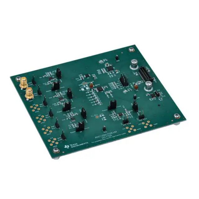
-
ADC128S102EVM
Texas Instruments
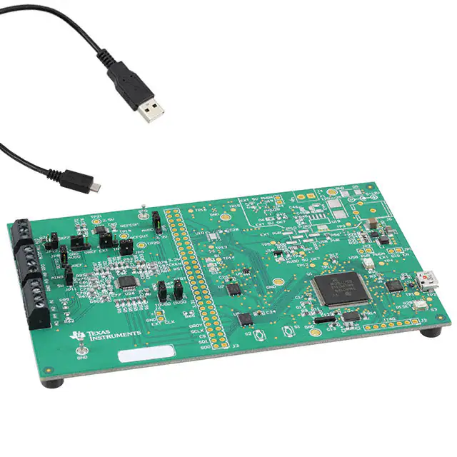
-
ADS124S08EVM
Texas Instruments
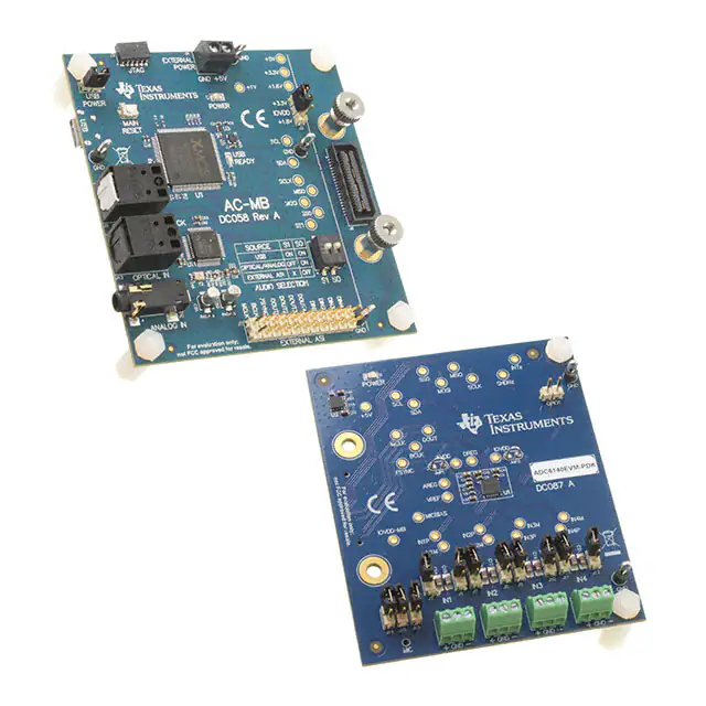
-
ADC6140EVM-PDK
Texas Instruments
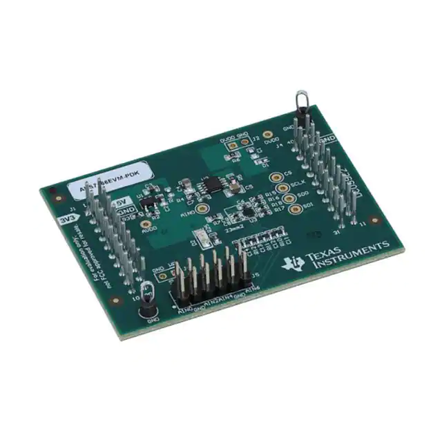
-
ADS7066EVM-PDK
Texas Instruments
Tech Hub

A practical engineering guide to 3.3V and 5V logic compatibility, input thresholds, resistor dividers, translator ICs, MOSFET level shifting, I2C pull-ups, timing limits and power-sequencing risks.

The 74HC595 uses push-pull logic outputs, while the TPIC6B595 uses 50 V open-drain DMOS sinks for higher-power loads. This guide compares timing, current limits, 3.3 V interfacing, load wiring, thermal…

The 74HC595 converts serial data into eight stable parallel outputs. This guide covers pin functions, shift and storage timing, OE and MR behavior, drive-current limits, cascading, voltage compatibilit…

A technical comparison of level-sensitive latches and edge-triggered flip-flops, covering timing windows, setup and hold limits, master–slave operation, time borrowing, race-through, HDL inference and…

A D latch stores one bit while Enable controls when data can pass. This reference covers gate-level operation, truth tables, transparency, setup and hold timing, LE versus OE, common ICs and practical …

An SR latch stores one bit through cross-coupled feedback. This engineering reference covers NOR and NAND implementations, truth tables, forbidden-state recovery, gated operation, switch debouncing, fa…

Latch circuits retain one bit through feedback. This technical reference covers SR and D latches, truth tables, transparency, timing limits, latch-versus-flip-flop behavior, applications and common log…

An engineering guide to LED driver operation, constant-current and constant-voltage outputs, linear and switching topologies, dimming, IC selection, calculations, replacement compatibility, and fault c…

Operational amplifier guide covering op amp basics, feedback, ideal vs real op amps, common configurations, buffer circuits, offset, bias current, gain-bandwidth, slew rate, rail-to-rail limits and sel…

Jumper cables guide covering safe connection order, red and black clamp placement, final ground connection, cable gauge, length, clamp quality, copper vs CCA cables, jump starter comparison and battery…


