
 My Inquiry
 My Account


NXP Semiconductors ADC1115S125HN/C1:5
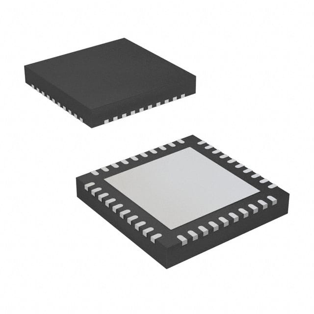
- Part No.:
- ADC1115S125HN/C1:5
- Manufacturer:
- NXP Semiconductors
- Category:
- Analog to Digital Converters (ADC)
- Package:
- 40-VFQFN Exposed Pad
- Datasheet:
-
 ADC1115S125HN/C1:5.pdf
- Description:
- IC ADC 11BIT PIPELINED 40HVQFN
- Quantity:
- Payment:

- Shipping:

Inventory:1,745
Please send an inquiry. Send us your inquiry, and we will respond immediately.
Product details
Overview
ADC1115S125HN/C1 from NXP Semiconductors is a single-channel 11-bit pipelined analog-to-digital converter optimized for high dynamic performance and low power at 125 Msps sample rate. It features an integrated input buffer, supports both CMOS and LVDS DDR digital outputs, and delivers 66.5 dBFS SNR and 86 dBc SFDR up to 170 MHz input frequency - ideal for high-IF communications and ultrasound signal acquisition.
For engineers reviewing the ADC1115S125HN/C1 datasheet, ADC1115S125HN/C1 pinout, ADC1115S125HN/C1 application, or ADC1115S125HN/C1 equivalent, key selection considerations include its programmable 1–2 Vp-p full-scale range, SPI-configurable output standard/format, duty cycle stabilizer, and HVQFN40 package with dual-mode (CMOS/LVDS DDR) pin compatibility across the ADC1015S/1215S/1415S families.
Technical Context
The ADC1115S125HN/C1 employs a 11-bit pipelined architecture with on-chip error correction ensuring zero missing codes. Its integrated input buffer isolates the S/H stage from source impedance variations, maintaining consistent 600 MHz input bandwidth and stable performance from baseband to ≥170 MHz.
It accepts differential LVPECL or single-ended LVCMOS clock inputs, includes a duty cycle stabilizer (DCS_EN), and supports flexible reference configuration - internal (SPI-programmable 0 to −6 dB gain steps) or external (0.5–1 V on VREF) - enabling precise full-scale tuning between 1 Vp-p and 2 Vp-p.
Key Specifications
| Parameter | Value and Actual Design Meaning |
|---|---|
| Resolution & Speed | 11-bit, 125 Msps - enables high-fidelity digitization of wideband IF signals in SDR and medical imaging systems. |
| Dynamic Performance | 66.5 dBFS SNR, 86 dBc SFDR at 70 MHz - meets demanding spectral purity requirements for digital predistortion and spectral analysis. |
| Input Bandwidth | 600 MHz - supports direct sampling of high-IF signals without external amplification or filtering. |
| Power Dissipation | 840 mW total (including analog input buffer) at 125 Msps - balances performance and thermal management in compact RF front-ends. |
| Output Interface | Configurable CMOS or LVDS DDR - LVDS DDR reduces EMI and supports longer trace routing; CMOS simplifies interface to FPGA I/O banks. |
| Reference Flexibility | Programmable 1–2 Vp-p full-scale via SPI or pin control - allows optimization for varying signal chain gain distribution and noise floor targets. |
| Operating Temperature | −40 °C to +85 °C - qualified for industrial and portable instrumentation environments. |
Pinout & Package
HVQFN40 (SOT618-6), 6 × 6 × 0.85 mm, thermally enhanced no-lead package with exposed thermal pad. Pin numbering follows standard HVQFN top-view orientation (pin 1 index area bottom-left).
| Pin/Terminal | Circuit Role | Design Meaning |
|---|---|---|
| INP / INM | Differential analog input | High-Z, 600 MHz bandwidth input pair; internally biased; requires AC coupling and common-mode termination via VCM. |
| CLKP / CLKM | Differential clock input | Accepts LVPECL or sine/LVCMOS (single-ended); duty cycle stabilizer improves jitter tolerance when enabled. |
| VDDA5V / VDDA3V / VDDO | Analog & output supply rails | Separate 5 V (core), 3 V (analog bias), and 1.8–3.6 V (output) supplies enable independent noise isolation and logic-level flexibility. |
| SDIO/ODS / SCLK/DFS / CS | SPI interface pins | Configures output standard (CMOS/LVDS DDR), data format (offset binary/two's complement/gray), and reference mode; supports pin-control fallback. |
| DAV / DAVP / DAVM | Data valid strobe | CMOS: single-ended DAV; LVDS DDR: differential DAVP/DAVM - synchronizes sampled data capture in high-speed FPGA receivers. |
| OTR | Out-of-range indicator | Active-HIGH flag signaling input overrange condition - enables real-time clipping detection and AGC feedback loops. |
Key Features
| Feature | Design Value |
|---|---|
| Integrated input buffer | Eliminates kickback-induced distortion and maintains constant low input capacitance (1.3 pF), simplifying driver design across 600 MHz bandwidth. |
| SPI programmable full-scale | Adjusts input range from 1 Vp-p to 2 Vp-p in 1 dB steps - enables optimal ADC utilization without external gain stages. |
| Duty cycle stabilizer (DCS) | Compensates clock duty cycle deviations (30–70 %), reducing aperture jitter and preserving SNR/SFDR in noisy clock domains. |
| Flexible output interface | Hardware-selectable CMOS or LVDS DDR outputs - supports legacy FPGA interfaces or high-noise immunity in dense RF layouts. |
| Zero missing codes guarantee | Guaranteed monotonicity and linearity (±0.1 LSB DNL) over full temperature range - essential for precision measurement and calibration-critical applications. |
| Low-power operating modes | Power-down (2 mW) and Sleep (40 mW) modes - reduce system standby power in battery-powered portable instrumentation. |
Applications
| Wireless Base Station IF Digitization | Ultrasound Beamforming Front-End |
|---|---|
|
Use Scenario: Digitizing 100–200 MHz intermediate frequency signals from mixer outputs in macro/microcell BTS transceivers. IC Role / Device Role / Timing Role: High-speed ADC capturing wideband IF samples for digital downconversion and channelization in FPGA-based radio processing units. Use Value: 600 MHz input bandwidth and 170 MHz usable Nyquist zone enable direct IF sampling, eliminating analog filters and local oscillator stages. |
Use Scenario: Acquiring echo return signals from phased-array transducers in portable ultrasound scanners. IC Role / Device Role / Timing Role: Channel ADC in multi-channel receive beamformer ASICs, synchronized via low-jitter LVDS DDR interface to FPGA correlators. Use Value: Integrated input buffer ensures consistent gain/phase response across channels, critical for coherent beam synthesis and image resolution. |
| Software Defined Radio (SDR) Receiver | Digital Predistortion (DPD) Feedback Loop |
|
Use Scenario: Wideband spectrum monitoring and adaptive modulation reception in field-deployable SDR platforms. IC Role / Device Role / Timing Role: Primary ADC feeding real-time FFT engines and demodulators; configured in LVDS DDR mode for noise-immune data transfer. Use Value: 66.5 dBFS SNR and 86 dBc SFDR support high-order QAM demodulation (e.g., 256-QAM) under crowded spectral conditions. |
Use Scenario: Capturing PA output signals for real-time nonlinear modeling and inverse predistortion coefficient update. IC Role / Device Role / Timing Role: Feedback-path ADC sampling PA output at 125 Msps to generate time-aligned complex baseband error signals. Use Value: Programmable 1–2 Vp-p full-scale adapts to varying PA output power levels, maximizing dynamic range utilization in closed-loop DPD. |
Equivalent & Alternatives
The following parts are listed as comparable options for similar high-speed ADC applications.
| Alternative Part | Technical Difference | Application Difference | Selection Advice |
|---|---|---|---|
| ADC1215S125HN/C1 | 12-bit resolution, identical 125 Msps speed, same HVQFN40 package and pinout; higher power (920 mW). | Better ENOB (11.2 bits vs. 10.7 bits) suits applications requiring finer amplitude quantization, e.g., high-fidelity spectral analysis. | Select when 12-bit resolution justifies ~10 % higher power and cost; drop-in replacement with no layout change. |
| ADS5272IPFP | Texas Instruments 12-bit, 65 Msps quad-channel ADC; different package (HTQFP64), no LVDS DDR, SPI not supported. | Lower sample rate but multi-channel integration reduces board space in channel-dense systems like MRI front-ends. | Choose for multi-channel parallel sampling where per-channel speed < 125 Msps is acceptable and board area is constrained. |
Compared with ADC1115S125HN/C1, the ADC1215S125HN/C1 offers higher resolution at identical speed and footprint, while the ADS5272IPFP trades speed for channel density and simplified interface - making each suitable for distinct system-level trade-offs in RF, medical, or test equipment.
Availability
ADC1115S125HN/C1 is available at Aetrix Electronics and suitable for wireless infrastructure, portable medical imaging, and software-defined radio applications requiring stable component supply, long-term lifecycle assurance, and traceable sourcing.
Supply support for ADC1115S125HN/C1 includes scheduled delivery planning, volume procurement assistance, BOM continuity management, traceable sourcing, and lifecycle availability coordination for OEM customers, industrial embedded developers, connected-device designers, and electronics production programs.
Manufacturer
NXP Semiconductors is a global semiconductor leader focused on secure connectivity solutions for automotive, industrial, and communication markets.
The ADC1115S125HN/C1 belongs to NXP's high-speed data converter family designed specifically for demanding RF and IF digitization in communications infrastructure, medical ultrasound, and test equipment - emphasizing dynamic performance, low power, and flexible interface configurability.
FAQ
What is the maximum input frequency supported by the ADC1115S125HN/C1?
The ADC1115S125HN/C1 maintains specified dynamic performance (66.5 dBFS SNR, 86 dBc SFDR) up to 170 MHz input frequency, with a 600 MHz small-signal input bandwidth. This enables direct sampling of high-IF signals without external bandpass filtering, supporting architectures like zero-IF and high-IF in wireless receivers and spectrum analyzers.
Does the ADC1115S125HN/C1 support both CMOS and LVDS DDR output modes simultaneously?
No, the ADC1115S125HN/C1 supports either CMOS or LVDS DDR output mode - selected at power-up via pin ODS (Pin control mode) or via SPI register (SPI control mode). The two modes use mutually exclusive pin assignments (e.g., D10–D0 vs. D9_D10_P/M), so hardware configuration must match the chosen interface standard.
How is the full-scale input range configured on the ADC1115S125HN/C1?
The ADC1115S125HN/C1 full-scale range is configurable from 1 Vp-p to 2 Vp-p using either SPI (INTREF[2:0] bits with INTREF_EN = 1) or pin-based programming (SENSE and VREF pins). Internal reference modes yield fixed 1 Vp-p or 2 Vp-p; SPI enables 7 discrete steps (0 to −6 dB), allowing precise matching to signal chain gain distribution.
What clock input standards does the ADC1115S125HN/C1 accept?
The ADC1115S125HN/C1 accepts differential LVPECL, differential sine wave, or single-ended LVCMOS clock inputs. LVCMOS drive requires connecting the unused clock pin (CLKM or CLKP) to ground via a capacitor. The internal duty cycle stabilizer (DCS_EN) compensates for clock asymmetry, improving jitter tolerance in noisy environments.
Is the ADC1115S125HN/C1 pin-compatible with other devices in the ADC1x15S series?
Yes, the ADC1115S125HN/C1 is pin-compatible with the ADC1015S, ADC1215S, and ADC1415S series in the same HVQFN40 package. This enables scalable resolution migration (10/11/12/14-bit) within identical PCB layouts, simplifying design reuse and platform evolution across performance tiers.
ADC1115S125HN/C1:5 Specifications
- Product attributes
- Attribute value
- Manufacturer:
- NXP Semiconductors
- Series:
- -
- Package/Case:
- 40-VFQFN Exposed Pad
- Packaging:
- Tray
- Product Status:
- Obsolete
- Number of Bits:
- 11
- Sampling Rate (Per Second):
- 125M
- Number of Inputs:
- 1
- Input Type:
- Differential, Single Ended
- Data Interface:
- LVDS - Parallel, Parallel
- Configuration:
- S/H-ADC
- Ratio - S/H:ADC:
- 1:1
- Number of A/D Converters:
- 1
- Architecture:
- Pipelined
- Reference Type:
- External, Internal
- Voltage - Supply, Analog:
- 2.85V ~ 3.4V, 5V
- Voltage - Supply, Digital:
- 1.65V ~ 3.6V
- Features:
- -
- Operating Temperature:
- -40°C ~ 85°C
- Supplier Device Package:
- 40-HVQFN (6x6)
- Mounting Type:
- Surface Mount
- Grade:
- -
- Qualification:
- -
ADC1115S125HN/C1:5 FAQ
1.How can I place an order for ADC1115S125HN/C1:5 through Aetrix?
Please submit a Request for Quotation (RFQ) for ADC1115S125HN/C1:5 on Aetrix. Our sales agent will provide a competitive quotation and guide you through the order confirmation once you accept the terms.
2.Are the price and stock information for ADC1115S125HN/C1:5 reliable?
The price and inventory of ADC1115S125HN/C1:5 are updated periodically and may fluctuate due to market conditions. Stock and pricing data are typically refreshed every 24 hours. Quotation validity for ADC1115S125HN/C1:5 is usually 5 days.
3.What payment methods are accepted for ADC1115S125HN/C1:5?
We accept Wire Transfer, PayPal, Credit Card, Western Union, MoneyGram, and Escrow for ADC1115S125HN/C1:5 transactions.
Note: Certain payment methods may incur a processing fee.
4.How is shipping managed for ADC1115S125HN/C1:5?
ADC1115S125HN/C1:5 orders can be shipped via leading logistics carriers, including DHL, UPS, FedEx, TNT, or Registered Mail.
Once your ADC1115S125HN/C1:5 order is processed, you will receive an email with the shipment details and tracking number.
Note: Tracking information may take up to 24 hours to appear. Express delivery typically takes 3–5 business days.
5.How can I obtain technical support or documentation for ADC1115S125HN/C1:5?
For technical support, including ADC1115S125HN/C1:5 datasheets, pinout diagrams, or application guidance, please contact our engineering support team. They can provide detailed documentation and assistance for your ADC1115S125HN/C1:5 requirements.
6.How does Aetrix verify that ADC1115S125HN/C1:5 is sourced from the original manufacturer or authorized distributors?
All ADC1115S125HN/C1:5 products on Aetrix are procured from qualified distributors and authorized channels. Our dedicated quality assurance team conducts strict verification, including traceability checks and, if necessary, third-party testing. This ensures that ADC1115S125HN/C1:5 meets industry standards.
7.What is the process for return or replacement of ADC1115S125HN/C1:5?
All ADC1115S125HN/C1:5 units undergo pre-shipment inspection (PSI). If there is an issue with ADC1115S125HN/C1:5, returns or replacements are accepted under the following conditions:
1.Quantity discrepancies, incorrect items, or visible external defects (such as breakage or corrosion), acknowledged by Aetrix.
2.The issue is reported within 90 days of delivery.
3.The ADC1115S125HN/C1:5 part is unused and in its original packaging.
Return procedure for ADC1115S125HN/C1:5:
1.Submit a request within 90 days.
2.Obtain a Return Material Authorization (RMA) from Aetrix.
ADC1115S125HN/C1:5 Tags
-
ADC081C021CIMKX/NOPB
Texas Instruments

-
MCP3021A5T-E/OT
Microchip Technology
-
TLA2024IRUGR
Texas Instruments
-
MCP3221A5T-E/OT
Microchip Technology
-
MCP3221A5T-I/OT
Microchip Technology
-
MCP3221A4T-E/OT
Microchip Technology
-
MCP3221A6T-E/OT
Microchip Technology
-
MCP3221A0T-E/OT
Microchip Technology
-
MCP3221A1T-E/OT
Microchip Technology

-
ADC121S021CIMFX/NOPB
Texas Instruments

-
MCP3001-I/MS
Microchip Technology

-
MCP3001-I/SN
Microchip Technology
Tech Hub

A practical engineering guide to 3.3V and 5V logic compatibility, input thresholds, resistor dividers, translator ICs, MOSFET level shifting, I2C pull-ups, timing limits and power-sequencing risks.

The 74HC595 uses push-pull logic outputs, while the TPIC6B595 uses 50 V open-drain DMOS sinks for higher-power loads. This guide compares timing, current limits, 3.3 V interfacing, load wiring, thermal…

The 74HC595 converts serial data into eight stable parallel outputs. This guide covers pin functions, shift and storage timing, OE and MR behavior, drive-current limits, cascading, voltage compatibilit…

A technical comparison of level-sensitive latches and edge-triggered flip-flops, covering timing windows, setup and hold limits, master–slave operation, time borrowing, race-through, HDL inference and…

A D latch stores one bit while Enable controls when data can pass. This reference covers gate-level operation, truth tables, transparency, setup and hold timing, LE versus OE, common ICs and practical …

An SR latch stores one bit through cross-coupled feedback. This engineering reference covers NOR and NAND implementations, truth tables, forbidden-state recovery, gated operation, switch debouncing, fa…

Latch circuits retain one bit through feedback. This technical reference covers SR and D latches, truth tables, transparency, timing limits, latch-versus-flip-flop behavior, applications and common log…

An engineering guide to LED driver operation, constant-current and constant-voltage outputs, linear and switching topologies, dimming, IC selection, calculations, replacement compatibility, and fault c…

Operational amplifier guide covering op amp basics, feedback, ideal vs real op amps, common configurations, buffer circuits, offset, bias current, gain-bandwidth, slew rate, rail-to-rail limits and sel…

Jumper cables guide covering safe connection order, red and black clamp placement, final ground connection, cable gauge, length, clamp quality, copper vs CCA cables, jump starter comparison and battery…


