
 My Inquiry
 My Account


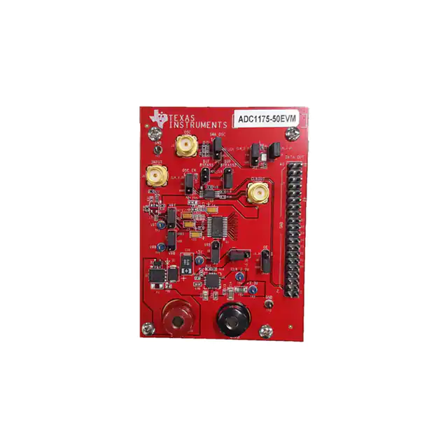
Texas Instruments ADC1175-50EVM
- Part No.:
- ADC1175-50EVM
- Manufacturer:
- Texas Instruments
- Package:
- Datasheet:
-
 ADC1175-50EVM.pdf
- Description:
- EVAL MODULE FOR ADC1175
- Quantity:
- Payment:

- Shipping:

Inventory:2,549
Please send an inquiry. Send us your inquiry, and we will respond immediately.
Product details
Overview
ADC1175-50EVM from Texas Instruments is an evaluation module designed exclusively for the ADC1175-50 8-bit, 50 MSPS analog-to-digital converter. It provides a complete, ready-to-use hardware platform with onboard clock generation, programmable LDO voltage regulation, level-shifting CMOS output buffer, and configurable analog input path - enabling rapid performance validation of dynamic parameters including SNR (44 dBFS) and SFDR (51 dBFS) at full sample rate.
For engineers reviewing the ADC1175-50EVM datasheet, ADC1175-50EVM pinout, ADC1175-50EVM application, or ADC1175-50EVM equivalent, this EVM supports direct integration with TI's TSW1400EVM data capture board, requires Windows-based HSDC Pro software, and delivers validated quick-start measurements using a 5-MHz band-pass filtered +10 dBm analog input signal with JP11 shunted to positions 1–2.
Technical Context
The ADC1175-50EVM implements a dedicated hardware interface for the ADC1175-50 IC, featuring a user-selectable 20-MHz onboard crystal oscillator (JP2 = 1–2) or external 20-MHz clock input (JP2 = 2–3), and supports coherent sampling via frequency-locked clock/analog sources. Its analog front-end includes an OPA830 op amp configured for 1.6-V DC offset and reference voltages of 2.6 V (VRT) and 0.6 V (VRB) when JP6 and JP9 are shunted 2–3.
Jumper JP11 (shunt 1–2) configures the input data voltage level specifically for ADC1175-50EVM operation, while JP10 (2–3) enables the CMOS output data buffer. The module interfaces to the TSW1400EVM via a 20-pin CMOS_INTERFACE header (J1), supporting direct connection of all 8 data bits, clock, and control signals without level translation.
Key Specifications
| Parameter | Value and Actual Design Meaning |
|---|---|
| Target Device | ADC1175-50 8-bit, 50 MSPS analog-to-digital converter |
| Sampling Rate Support | Validated at 50 MSPS using HSDC Pro with "ADC1175-50_cmos" firmware |
| Dynamic Performance | SNR = 44 dBFS, SFDR = 51 dBFS (measured per Table 3, SNAU224) |
| Analog Input Path | 5-MHz band-pass filtered +10 dBm signal applied to J6; OPA830 offset = 1.6 V |
| Reference Voltage | 2.6 V (VRT) and 0.6 V (VRB) set by JP6/JP9 shunted 2–3 |
| Power Supply | +5 VDC, ≥3 A via banana jack connectors (J4/J5) |
| Interface Standard | CMOS-level parallel digital output (8-bit data + clock + control) to TSW1400EVM |
Availability
ADC1175-50EVM is available at Aetrix Electronics and suitable for high-speed data converter evaluation, RF receiver prototyping, and mixed-signal test system development requiring stable component supply and TI-validated reference designs.
Supply support for ADC1175-50EVM includes scheduled delivery planning, volume procurement assistance, BOM continuity management, traceable sourcing, and lifecycle availability coordination for OEM customers, industrial embedded developers, connected-device designers, and electronics production programs.
Manufacturer
Texas Instruments is a global semiconductor company delivering analog and embedded processing solutions, with leadership in data converters, power management, and interface technologies.
The ADC1175-50EVM belongs to TI's high-speed ADC evaluation module family, engineered to accelerate characterization and system integration of low-power, medium-speed ADCs in communications, instrumentation, and digital receiver applications.
FAQ
What is the primary function of the ADC1175-50EVM?
The ADC1175-50EVM is a dedicated evaluation module for the ADC1175-50 analog-to-digital converter. It provides a complete test platform-including clocking, analog input conditioning, voltage regulation, and CMOS output buffering-to validate dynamic performance metrics such as SNR and SFDR at 50 MSPS. The ADC1175-50EVM is not a standalone product but a TI-qualified hardware tool for design-in verification and system-level testing of the ADC1175-50 IC.
Which software and host hardware are required to operate the ADC1175-50EVM?
The ADC1175-50EVM requires Texas Instruments' High-Speed Data Converter Pro (HSDC Pro) software running on a Windows PC (XP or later), along with the TSW1400EVM data capture board. The ADC1175-50EVM connects directly to the TSW1400EVM via its CMOS_INTERFACE header (J1), and firmware selection must be set to "ADC1175-50_cmos" within HSDC Pro to ensure correct timing, register mapping, and analysis settings for the ADC1175-50EVM configuration.
How is the input voltage level configured on the ADC1175-50EVM?
The input data voltage level on the ADC1175-50EVM is configured using jumper JP11: shunting pins 1–2 selects the setting specific to the ADC1175-50 variant, as documented in Table 5 of the SNAU224 User's Guide. This jumper ensures proper logic-level alignment between the ADC1175-50's CMOS outputs and the TSW1400EVM's input receivers. Leaving JP11 unshunted or in any other position invalidates the ADC1175-50EVM's operational configuration.
What are the key hardware dependencies for achieving the published 44 dBFS SNR on the ADC1175-50EVM?
Achieving the published 44 dBFS SNR on the ADC1175-50EVM requires strict adherence to the quick-start setup: a +10 dBm, 5-MHz analog input signal passed through a ≥60-dB harmonic attenuation band-pass filter, applied to J6; JP11 shunted 1–2; JP2 shunted 1–2 for internal 20-MHz clock; and use of the HSDC Pro "ADC1175-50_cmos" firmware with "50M" entered in the ADC Output Data Rate field. Deviations-such as incorrect filter bandwidth, excessive input amplitude (> –1 dBFS), or mismatched firmware-degrade measured SNR.
Can the ADC1175-50EVM be used with external clock sources, and how is that configured?
Yes, the ADC1175-50EVM supports external clocking: shunt JP2 to positions 2–3 and remove the jumper from JP7 to disable the onboard oscillator. Then apply a clean 20-MHz, 1-dBm clock signal to connector J3. The external source must exhibit low phase noise (< 500 fs jitter, 20 kHz–20 MHz offset) to maintain the ADC1175-50EVM's specified dynamic performance. Clock coherence with the analog input source is recommended for optimal SNR, and narrow-band filtering of the external clock is advised per Section 3.1 of SNAU224.
ADC1175-50EVM Specifications
- Product attributes
- Attribute value
- Manufacturer:
- Texas Instruments
- Series:
- -
- Packaging:
- Bulk
- Product Status:
- Obsolete
- Number of A/D Converters:
- 1
- Number of Bits:
- 8
- Sampling Rate (Per Second):
- 50M
- Data Interface:
- Parallel
- Input Range:
- -
- Power (Typ) @ Conditions:
- -
- Utilized IC / Part:
- ADC1175-50
- Contents:
- Board(s)
ADC1175-50EVM FAQ
1.How can I place an order for ADC1175-50EVM through Aetrix?
Please submit a Request for Quotation (RFQ) for ADC1175-50EVM on Aetrix. Our sales agent will provide a competitive quotation and guide you through the order confirmation once you accept the terms.
2.Are the price and stock information for ADC1175-50EVM reliable?
The price and inventory of ADC1175-50EVM are updated periodically and may fluctuate due to market conditions. Stock and pricing data are typically refreshed every 24 hours. Quotation validity for ADC1175-50EVM is usually 5 days.
3.What payment methods are accepted for ADC1175-50EVM?
We accept Wire Transfer, PayPal, Credit Card, Western Union, MoneyGram, and Escrow for ADC1175-50EVM transactions.
Note: Certain payment methods may incur a processing fee.
4.How is shipping managed for ADC1175-50EVM?
ADC1175-50EVM orders can be shipped via leading logistics carriers, including DHL, UPS, FedEx, TNT, or Registered Mail.
Once your ADC1175-50EVM order is processed, you will receive an email with the shipment details and tracking number.
Note: Tracking information may take up to 24 hours to appear. Express delivery typically takes 3–5 business days.
5.How can I obtain technical support or documentation for ADC1175-50EVM?
For technical support, including ADC1175-50EVM datasheets, pinout diagrams, or application guidance, please contact our engineering support team. They can provide detailed documentation and assistance for your ADC1175-50EVM requirements.
6.How does Aetrix verify that ADC1175-50EVM is sourced from the original manufacturer or authorized distributors?
All ADC1175-50EVM products on Aetrix are procured from qualified distributors and authorized channels. Our dedicated quality assurance team conducts strict verification, including traceability checks and, if necessary, third-party testing. This ensures that ADC1175-50EVM meets industry standards.
7.What is the process for return or replacement of ADC1175-50EVM?
All ADC1175-50EVM units undergo pre-shipment inspection (PSI). If there is an issue with ADC1175-50EVM, returns or replacements are accepted under the following conditions:
1.Quantity discrepancies, incorrect items, or visible external defects (such as breakage or corrosion), acknowledged by Aetrix.
2.The issue is reported within 90 days of delivery.
3.The ADC1175-50EVM part is unused and in its original packaging.
Return procedure for ADC1175-50EVM:
1.Submit a request within 90 days.
2.Obtain a Return Material Authorization (RMA) from Aetrix.
ADC1175-50EVM Tags
-
1083
Adafruit Industries LLC
-
1085
Adafruit Industries LLC
-
ADS7038Q1EVM-PDK
Texas Instruments
-
ADS8688EVM-PDK
Texas Instruments
-
EVAL-AD7606C18FMCZ
Analog Devices Inc.
-
ADS1232REF
Texas Instruments
-
EVAL-AD4134FMCZ
Analog Devices Inc.
-
EVAL-AD7768FMCZ
Analog Devices Inc.
-
ADC128S102EVM
Texas Instruments
-
ADS124S08EVM
Texas Instruments
-
ADC6140EVM-PDK
Texas Instruments
-
ADS7066EVM-PDK
Texas Instruments
Tech Hub

A practical engineering guide to 3.3V and 5V logic compatibility, input thresholds, resistor dividers, translator ICs, MOSFET level shifting, I2C pull-ups, timing limits and power-sequencing risks.

The 74HC595 uses push-pull logic outputs, while the TPIC6B595 uses 50 V open-drain DMOS sinks for higher-power loads. This guide compares timing, current limits, 3.3 V interfacing, load wiring, thermal…

The 74HC595 converts serial data into eight stable parallel outputs. This guide covers pin functions, shift and storage timing, OE and MR behavior, drive-current limits, cascading, voltage compatibilit…

A technical comparison of level-sensitive latches and edge-triggered flip-flops, covering timing windows, setup and hold limits, master–slave operation, time borrowing, race-through, HDL inference and…

A D latch stores one bit while Enable controls when data can pass. This reference covers gate-level operation, truth tables, transparency, setup and hold timing, LE versus OE, common ICs and practical …

An SR latch stores one bit through cross-coupled feedback. This engineering reference covers NOR and NAND implementations, truth tables, forbidden-state recovery, gated operation, switch debouncing, fa…

Latch circuits retain one bit through feedback. This technical reference covers SR and D latches, truth tables, transparency, timing limits, latch-versus-flip-flop behavior, applications and common log…

An engineering guide to LED driver operation, constant-current and constant-voltage outputs, linear and switching topologies, dimming, IC selection, calculations, replacement compatibility, and fault c…

Operational amplifier guide covering op amp basics, feedback, ideal vs real op amps, common configurations, buffer circuits, offset, bias current, gain-bandwidth, slew rate, rail-to-rail limits and sel…

Jumper cables guide covering safe connection order, red and black clamp placement, final ground connection, cable gauge, length, clamp quality, copper vs CCA cables, jump starter comparison and battery…


