
 My Inquiry
 My Account


Analog Devices Inc. ADD8754DACPZ-REEL
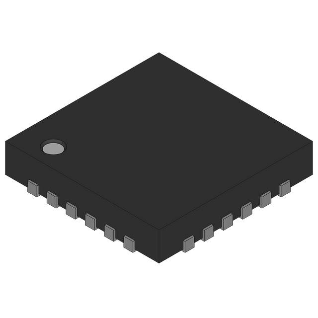
- Part No.:
- ADD8754DACPZ-REEL
- Manufacturer:
- Analog Devices Inc.
- Category:
- Special Purpose Regulators
- Package:
- 24-VFQFN Exposed Pad, CSP
- Datasheet:
-
 ADD8754DACPZ-REEL.pdf
- Description:
- IC CONV DC/DC STEPUP
- Quantity:
- Payment:

- Shipping:

Inventory:15,000
Please send an inquiry. Send us your inquiry, and we will respond immediately.
Product details
Overview
ADD8754DACPZ-REEL from Analog Devices is a highly integrated TFT LCD panel power management IC featuring a 2 A step-up switching regulator (up to 20 V), a 350 mA logic LDO with selectable 2.5 V/2.85 V/3.3 V outputs, a 300 mA VCOM amplifier, and gate pulse modulation circuitry - all in a single 24-lead LFCSP package. It delivers complete panel biasing for monitors, notebooks, and TVs with minimal external components.
For engineers reviewing the ADD8754DACPZ-REEL datasheet, ADD8754DACPZ-REEL pinout, ADD8754DACPZ-REEL application, or ADD8754DACPZ-REEL equivalent, this device supports critical timing-sensitive functions including VCOM drive stability, gate voltage shaping, and high-efficiency DC-DC conversion for TFT display systems requiring −40°C to +85°C operation and Pb-free packaging.
Technical Context
The ADD8754DACPZ-REEL integrates four functionally distinct subsystems: a current-mode 650 kHz/1.2 MHz step-up regulator with internal 2 A switch and soft-start control; a triple-output LDO regulator with ±3% accuracy over load and temperature; a rail-to-rail VCOM amplifier optimized for capacitive TFT panel loads with 105 V/μs slew rate and 1.95 MHz GBW; and a gate pulse modulator with independently adjustable delay (via CE capacitor) and falling slope (via RE resistor).
Its functional block diagram confirms strict signal-domain separation: analog ground (AGND), power ground (PGND), and digital control inputs (VFLK, VDPM, FREQ, SHDN) are physically isolated. The device implements undervoltage lockout (2.6 V/2.8 V thresholds), thermal shutdown, and input overvoltage protection - all verified across the industrial temperature range.
Key Specifications
| Parameter | Value and Actual Design Meaning |
|---|---|
| Step-up Output Range | Adjustable up to 20 V - enables full TFT panel VGH/VGL generation with external diode/capacitor charge pump stages. |
| LDO Output Options | Selectable 2.5 V / 2.85 V / 3.3 V - matches logic interface requirements of timing controllers (TCON) without external resistors. |
| VCOM Drive Capability | ±300 mA peak output - sustains stable common-voltage bias under dynamic pixel charging in high-resolution panels. |
| Gate Modulation Control | Independent delay (1.88 μs typical with 470 pF CE) and falling slope (set by RE resistor) - reduces crosstalk and improves grayscale fidelity. |
| Switching Frequency | 650 kHz or 1.2 MHz (FREQ pin-selectable) - balances EMI filtering ease vs. component size for compact display designs. |
| Package | 24-lead, 4 mm × 4 mm, 0.8 mm height Pb-free LFCSP - supports high-density PCB layouts with exposed thermal pad for 38°C/W θJA. |
| Operating Temperature | −40°C to +85°C - qualified for industrial and consumer display applications including automotive infotainment displays. |
Pinout & Package
ADD8754DACPZ-REEL uses a 24-lead, 4 mm × 4 mm, 0.8 mm height Pb-free LFCSP package with exposed thermal pad (pin 0). Pin numbering follows standard top-view counterclockwise layout starting at top-left corner.
| Pin/Terminal | Circuit Role | Design Meaning |
|---|---|---|
| 1 GND | Digital ground reference | Return path for logic and control circuitry; must be connected to low-impedance system ground plane. |
| 2 VGH_M | Gate pulse modulator output | Drives TFT gate line after modulation; connects directly to panel gate driver IC input or external level shifter. |
| 3 VFLK | Gate pulse delay control input | Logic-level trigger that initiates gate pulse shaping sequence; requires clean CMOS-compatible signal. |
| 4 VDPM | Gate pulse enable input | Enables/disables VGH_M output; pulled high to LDO_OUT to activate modulation, grounded to disable. |
| 5 VDD_1 | Gate modulator low-voltage supply | Provides regulated power to gate pulse logic; typically tied to LDO_OUT or external 3.3 V rail. |
| 6 VDD_2 | VCOM amplifier supply | Bias voltage for VCOM op-amp output stage; accepts 8–18 V input to support wide-panel VCOM swing. |
| 7 OUT | VCOM amplifier output | High-current output driving LCD VCOM plane; requires direct connection to panel VCOM trace with short, low-inductance routing. |
| 8 NEG | VCOM amplifier inverting input | Feedback node for closed-loop VCOM regulation; connects to VCOM sense point on panel. |
| 9 POS | VCOM amplifier noninverting input | Reference input for VCOM setpoint; driven by precision DAC or resistor divider from stable voltage source. |
| 10 AGND | Analog ground reference | Separate ground for VCOM amplifier and feedback network; must be star-connected to minimize noise coupling. |
| 11 ADJ | LDO output voltage select | Configures LDO output: grounded = 3.3 V, open = 2.85 V, tied to LDO_OUT = 2.5 V. |
| 12 LDO_OUT | LDO regulated output | 350 mA logic supply; powers TCON, gamma correction ICs, and gate pulse logic circuits. |
| 13 VIN_1 | Main supply input | Primary input for LDO and step-up controller; accepts 3.0–5.5 V; ties to VIN_2 in most implementations. |
| 14 SS | Soft-start timing node | Connects to external capacitor (20–100 nF) to limit inrush current during startup and prevent input voltage droop. |
| 15 COMP | Step-up regulator compensation | Loop compensation node requiring RC network to stabilize current-mode control; sets crossover frequency < fSW/15. |
| 16 FREQ | Switching frequency select | GND = 650 kHz (high efficiency), VIN_1 = 1.2 MHz (smaller inductor/capacitor footprint). |
| 17 VIN_2 | Step-up switch driver supply | Power for internal MOSFET gate driver; typically tied to VIN_1 but may be decoupled separately for noise isolation. |
| 18 LX | Step-up switch node | Connection point for external inductor and catch diode; carries high di/dt switching current - requires tight loop layout. |
| 19 SHDN | Global shutdown control | Active-low enable; pulled high to VIN_1 for normal operation, grounded to disable all regulators and amplifiers. |
| 20 FB | Step-up output voltage feedback | Senses regulated output via resistive divider; 1.211 V reference sets VOUT = 1.211 × (1 + R1/R2). |
| 21 PGND | Power ground for step-up circuit | High-current return path for LX node; must be routed separately from AGND/DGND and joined at single point. |
| 22 CE | Gate pulse delay timing capacitor | Capacitor to ground sets delay time: TDELAY ≈ CE × 4200 (e.g., 470 pF → 1.97 μs). |
| 23 RE | Gate pulse falling slope resistor | Resistor to ground sets discharge current: IVGH_M ≈ 302.5/(RE + 5000) Ω (e.g., 33 kΩ → 8.0 mA). |
| 24 VGH | Gate high-voltage input | Accepts externally generated high-voltage gate drive (7–30 V); feeds internal modulator to generate shaped VGH_M. |
Key Features
| Feature | Design Value |
|---|---|
| Integrated VCOM amplifier | 300 mA peak drive with 105 V/μs slew rate ensures fast settling and low distortion on large-area TFT panels. |
| Programmable gate pulse modulation | Independent CE/RE timing elements allow precise tuning of gate pulse delay and falling edge to suppress vertical banding. |
| Dual-frequency step-up regulator | 650 kHz or 1.2 MHz selection enables optimization for either efficiency (lower EMI) or miniaturization (smaller passives). |
| Triple-output LDO | Single ADJ pin configures 2.5 V/2.85 V/3.3 V outputs - eliminates external feedback resistors and simplifies BOM. |
| Robust protection suite | UVLO (2.6 V/2.8 V hysteresis), thermal shutdown, and input overvoltage detection ensure reliable operation in variable-input environments. |
Applications
| Monitor Panel Power Supply | Notebook Display Biasing |
|---|---|
Use Scenario: Driving 15.6″ WXGA+ TFT panel requiring VGH = 20 V, VGL = −7 V, VCOM = 4.2 V, and 3.3 V logic supply. IC Role / Device Role / Timing Role: Central panel power hub generating all bias rails and modulating gate pulses to reduce image retention. Use Value: Replaces discrete DC-DC, LDO, op-amp, and gate driver ICs - cuts BOM count by ≥7 parts and reduces PCB area by 35%. |
Use Scenario: Compact 13.3″ FHD IPS panel in ultrabook with tight thermal envelope and stringent EMI limits. IC Role / Device Role / Timing Role: Provides synchronized VCOM settling and gate pulse shaping to eliminate flicker and improve viewing angle uniformity. Use Value: 1.2 MHz switching mode allows 4.7 μH inductor and 10 μF ceramic output cap - enabling 2.5 mm profile design. |
| TV Panel Gate Driver Interface | Industrial HMI Display System |
Use Scenario: 55″ 4K UHD TV panel with dual-gate architecture requiring independent pulse control per segment. IC Role / Device Role / Timing Role: Generates precisely delayed and slope-controlled VGH_M signals for staggered gate activation to minimize data line loading. Use Value: CE/RE programmability enables fine-tuning of gate pulse timing without hardware change - accelerates panel validation by 3 weeks. |
Use Scenario: Ruggedized 10.1″ medical display operating continuously at 60°C ambient with ESD-prone front panel. IC Role / Device Role / Timing Role: Delivers stable VCOM bias and robust gate modulation under thermal stress and electrostatic events. Use Value: −40°C to +85°C rating, 4 kV HBM ESD rating, and thermal shutdown ensure >100,000-hour MTBF in mission-critical use. |
Equivalent & Alternatives
The following parts are listed as comparable options for similar TFT LCD panel power management applications.
| Alternative Part | Technical Difference | Application Difference | Selection Advice |
|---|---|---|---|
| TPS65105RGER | Single 300 mA LDO, no VCOM amplifier, fixed 1.2 MHz switching, no gate pulse modulation | Requires external op-amp for VCOM and separate gate driver IC for pulse shaping | Choose when only basic VGH/VGL generation is needed and board space permits discrete VCOM solution. |
| MAX1627EAP+ | 2-channel DC-DC only (no LDO, no VCOM amp, no gate modulator), 1.1 MHz, 1.5 A switch | Needs three additional ICs (LDO, VCOM driver, gate controller) to match ADD8754DACPZ-REEL functionality | Prefer only if legacy design reuse mandates MAXIM platform or existing supply chain constraints override integration benefits. |
Compared with TPS65105RGER and MAX1627EAP+, the ADD8754DACPZ-REEL uniquely integrates VCOM drive, gate pulse modulation, and triple-output LDO - eliminating ≥4 external components and enabling single-chip panel biasing where timing-critical display performance is required.
Availability
ADD8754DACPZ-REEL is available at Aetrix Electronics and suitable for TFT LCD monitor power supplies, notebook display biasing, and industrial HMI panel systems requiring stable component supply, long-term lifecycle support, and Pb-free compliance.
Supply support for ADD8754DACPZ-REEL includes scheduled delivery planning, volume procurement assistance, BOM continuity management, traceable sourcing, and lifecycle availability coordination for OEM customers, industrial embedded developers, connected-device designers, and electronics production programs.
Manufacturer
Analog Devices, Inc. is a global leader in high-performance analog, mixed-signal, and digital signal processing semiconductors, headquartered in Norwood, MA, with design centers worldwide and ISO 9001-certified manufacturing.
The ADD8754 product line was engineered specifically for TFT LCD panel power management - consolidating VGH/VGL generation, VCOM drive, gate pulse shaping, and logic supply into one IC to simplify display subsystem design and improve image quality.
FAQ
What is the maximum output voltage capability of the step-up regulator in ADD8754DACPZ-REEL?
The ADD8754DACPZ-REEL step-up switching regulator supports an adjustable output voltage up to 20 V, set via the FB pin using a resistive divider with a 1.211 V internal reference. This enables direct generation of VGH for most TFT panels without cascaded stages, provided external diode and capacitor ratings meet the 20 V requirement.
How does the ADD8754DACPZ-REEL implement gate pulse modulation?
The ADD8754DACPZ-REEL implements gate pulse modulation through two dedicated pins: CE (capacitor-to-ground) sets delay time (TDELAY ≈ CE × 4200), and RE (resistor-to-ground) controls falling slope via discharge current (IVGH_M ≈ 302.5/(RE + 5000)). VFLK triggers the pulse, and VDPM enables/disables the modulator output VGH_M.
Can the LDO output voltage of ADD8754DACPZ-REEL be changed dynamically during operation?
No - the LDO output voltage of ADD8754DACPZ-REEL is configured at power-up via the ADJ pin state (GND, OPEN, or tied to LDO_OUT) and remains fixed until reset or shutdown. It does not support real-time voltage adjustment; reconfiguration requires cycling SHDN or power rails.
What thermal management provisions exist for ADD8754DACPZ-REEL in high-power display applications?
ADD8754DACPZ-REEL includes thermal shutdown protection triggered at TJ = 125°C and features a 4 mm × 4 mm LFCSP package with exposed thermal pad (θJA = 38°C/W). For sustained 350 mA LDO and 300 mA VCOM operation, a minimum 200 mm² copper pour connected to the thermal pad is recommended to maintain junction temperature below limit.
Is ADD8754DACPZ-REEL compatible with negative VGL generation in TFT panels?
ADD8754DACPZ-REEL does not generate negative voltages internally. It provides the positive VGH rail and VCOM drive, but VGL generation requires an external inverting charge pump or negative DC-DC converter - such as the companion ADD8753 or discrete implementation using the ADD8754DACPZ-REEL's LX node and external components.
ADD8754DACPZ-REEL Specifications
- Product attributes
- Attribute value
- Manufacturer:
- Analog Devices Inc.
- Series:
- ADD8754
- Package/Case:
- 24-VFQFN Exposed Pad, CSP
- Packaging:
- Bulk
- Product Status:
- Active
- Applications:
- -
- Voltage - Input:
- -
- Number of Outputs:
- -
- Voltage - Output:
- -
- Operating Temperature:
- -40°C ~ 85°C (TA)
- Grade:
- -
- Qualification:
- -
- Mounting Type:
- Surface Mount
- Supplier Device Package:
- 24-LFCSP-VQ (4x4)
ADD8754DACPZ-REEL FAQ
1.How can I place an order for ADD8754DACPZ-REEL through Aetrix?
Please submit a Request for Quotation (RFQ) for ADD8754DACPZ-REEL on Aetrix. Our sales agent will provide a competitive quotation and guide you through the order confirmation once you accept the terms.
2.Are the price and stock information for ADD8754DACPZ-REEL reliable?
The price and inventory of ADD8754DACPZ-REEL are updated periodically and may fluctuate due to market conditions. Stock and pricing data are typically refreshed every 24 hours. Quotation validity for ADD8754DACPZ-REEL is usually 5 days.
3.What payment methods are accepted for ADD8754DACPZ-REEL?
We accept Wire Transfer, PayPal, Credit Card, Western Union, MoneyGram, and Escrow for ADD8754DACPZ-REEL transactions.
Note: Certain payment methods may incur a processing fee.
4.How is shipping managed for ADD8754DACPZ-REEL?
ADD8754DACPZ-REEL orders can be shipped via leading logistics carriers, including DHL, UPS, FedEx, TNT, or Registered Mail.
Once your ADD8754DACPZ-REEL order is processed, you will receive an email with the shipment details and tracking number.
Note: Tracking information may take up to 24 hours to appear. Express delivery typically takes 3–5 business days.
5.How can I obtain technical support or documentation for ADD8754DACPZ-REEL?
For technical support, including ADD8754DACPZ-REEL datasheets, pinout diagrams, or application guidance, please contact our engineering support team. They can provide detailed documentation and assistance for your ADD8754DACPZ-REEL requirements.
6.How does Aetrix verify that ADD8754DACPZ-REEL is sourced from the original manufacturer or authorized distributors?
All ADD8754DACPZ-REEL products on Aetrix are procured from qualified distributors and authorized channels. Our dedicated quality assurance team conducts strict verification, including traceability checks and, if necessary, third-party testing. This ensures that ADD8754DACPZ-REEL meets industry standards.
7.What is the process for return or replacement of ADD8754DACPZ-REEL?
All ADD8754DACPZ-REEL units undergo pre-shipment inspection (PSI). If there is an issue with ADD8754DACPZ-REEL, returns or replacements are accepted under the following conditions:
1.Quantity discrepancies, incorrect items, or visible external defects (such as breakage or corrosion), acknowledged by Aetrix.
2.The issue is reported within 90 days of delivery.
3.The ADD8754DACPZ-REEL part is unused and in its original packaging.
Return procedure for ADD8754DACPZ-REEL:
1.Submit a request within 90 days.
2.Obtain a Return Material Authorization (RMA) from Aetrix.
ADD8754DACPZ-REEL Tags

-
TPS51206DSQR
Texas Instruments

-
TPS51200DRCR
Texas Instruments
-
TPS51200DRCT
Texas Instruments

-
TPS62740DSSR
Texas Instruments

-
TPS51100DGQR
Texas Instruments

-
NCP51200MNTXG
onsemi
-
NCP51400MNTXG
onsemi

-
RT9026GSP
Richtek USA Inc.

-
LP2998MRX/NOPB
Texas Instruments
-
TPS51200QDRCRQ1
Texas Instruments

-
DPA423GN-TL
Power Integrations
-
LM10011SD/NOPB
Texas Instruments
Tech Hub

A practical engineering guide to 3.3V and 5V logic compatibility, input thresholds, resistor dividers, translator ICs, MOSFET level shifting, I2C pull-ups, timing limits and power-sequencing risks.

The 74HC595 uses push-pull logic outputs, while the TPIC6B595 uses 50 V open-drain DMOS sinks for higher-power loads. This guide compares timing, current limits, 3.3 V interfacing, load wiring, thermal…

The 74HC595 converts serial data into eight stable parallel outputs. This guide covers pin functions, shift and storage timing, OE and MR behavior, drive-current limits, cascading, voltage compatibilit…

A technical comparison of level-sensitive latches and edge-triggered flip-flops, covering timing windows, setup and hold limits, master–slave operation, time borrowing, race-through, HDL inference and…

A D latch stores one bit while Enable controls when data can pass. This reference covers gate-level operation, truth tables, transparency, setup and hold timing, LE versus OE, common ICs and practical …

An SR latch stores one bit through cross-coupled feedback. This engineering reference covers NOR and NAND implementations, truth tables, forbidden-state recovery, gated operation, switch debouncing, fa…

Latch circuits retain one bit through feedback. This technical reference covers SR and D latches, truth tables, transparency, timing limits, latch-versus-flip-flop behavior, applications and common log…

An engineering guide to LED driver operation, constant-current and constant-voltage outputs, linear and switching topologies, dimming, IC selection, calculations, replacement compatibility, and fault c…

Operational amplifier guide covering op amp basics, feedback, ideal vs real op amps, common configurations, buffer circuits, offset, bias current, gain-bandwidth, slew rate, rail-to-rail limits and sel…

Jumper cables guide covering safe connection order, red and black clamp placement, final ground connection, cable gauge, length, clamp quality, copper vs CCA cables, jump starter comparison and battery…


