
 My Inquiry
 My Account


Analog Devices Inc. ADF4193BCPZ-RL7
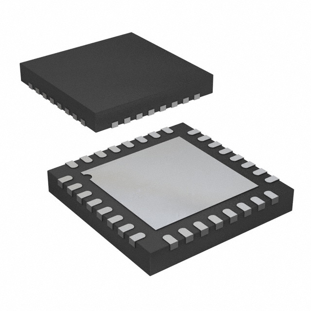
- Part No.:
- ADF4193BCPZ-RL7
- Manufacturer:
- Analog Devices Inc.
- Package:
- 32-WFQFN Exposed Pad, CSP
- Datasheet:
-
 ADF4193BCPZ-RL7.pdf
- Description:
- IC CLK/FREQ SYNTH 32LFCSP
- Quantity:
- Payment:

- Shipping:

Inventory:2,981
Please send an inquiry. Send us your inquiry, and we will respond immediately.
Product details
Overview
ADF4193BCPZ-RL7 from Analog Devices is a fast-settling, low-phase-noise fractional-N PLL frequency synthesizer designed for GSM/EDGE base station local oscillators. It delivers 5 µs frequency hop across the GSM band, 0.5° rms phase error at 2 GHz RF output, and −216 dBc/Hz phase noise figure of merit. Its architecture replaces ping-pong synthesizers in up/downconversion stages requiring sub-20 µs phase settling.
For engineers reviewing the ADF4193BCPZ-RL7 datasheet, ADF4193BCPZ-RL7 pinout, ADF4193BCPZ-RL7 application, or ADF4193BCPZ-RL7 equivalent, this device supports critical timing-critical RF subsystems where lock time, phase accuracy, and fractional spur suppression are design-determining factors - especially in automotive-qualified wireless infrastructure and instrumentation.
Technical Context
The ADF4193BCPZ-RL7 implements a Σ-Δ-based fractional interpolator with programmable modulus division (MOD register), enabling fine frequency resolution without integer boundary spurs. Its differential charge pump (ICP up/down matching ≤0.1%) and on-chip differential amplifier (7 nV/√Hz output noise) jointly enable stable VCO tuning with minimal added jitter.
Fast lock is achieved via dynamic loop bandwidth control: SW1/SW2/SW3 switches reconfigure the external loop filter during frequency transitions, while internal timers coordinate charge pump current scaling (6.6 mA high / 104 µA low) and phase detector frequency (up to 30 MHz). The 24-bit serial interface supports real-time phase programming and coherent phase look-up table updates.
Key Specifications
| Parameter | Value and Actual Design Meaning |
|---|---|
| RF Input Frequency | 0.4–3.5 GHz - supports direct injection from VCO outputs across GSM, DCS, PHS bands without external prescaler. |
| Phase Noise Figure of Merit | −216 dBc/Hz - enables ultra-low in-band phase noise floor in narrowband PLL designs with 500 kHz loop bandwidth. |
| Charge Pump Current Accuracy | ±5% typ - ensures precise N-divider ratio tracking and minimizes reference spurs in closed-loop operation. |
| Phase Settling Time | ≤20 µs - meets GSM time slot guard period requirement, eliminating need for dual-PLL architectures. |
| Output Phase Programmability | Digitally adjustable in 360°/MOD steps - allows coherent frequency hopping and I/Q calibration without hardware changes. |
| Automotive Qualification | −40°C to +105°C operating range (C version) - validated per AEC-Q100 for base station remote radio units in harsh environments. |
| Supply Voltages | AVDD/DVDD/SDVDD = 2.7–3.3 V; VP1/VP2 = 4.5–5.5 V; VP3 = 5.0–5.65 V - separates analog, digital, and high-voltage charge pump domains. |
Pinout & Package
ADF4193BCPZ-RL7 uses a 32-lead LFCSP (5 mm × 5 mm, 0.5 mm pitch) with exposed thermal pad. Pin functions are validated per Analog Devices Rev. G datasheet Figure 3 and Table 4.
| Pin/Terminal | Circuit Role | Design Meaning |
|---|---|---|
| RFIN+, RFIN− | Differential RF input | Accepts 0.4–3.5 GHz ac-coupled VCO signal; requires 100 pF bypass to AGND for impedance matching. |
| CPOUT+, CPOUT− | Differential charge pump output | Drives loop filter; matched ±0.1% current ensures minimal reference spurs and fast lock stability. |
| AIN+, AIN− | Differential amplifier inputs | Converts CPOUT differential voltage to single-ended VTUNE; 1.4–(VP3−0.3) V swing range. |
| AOUT | VCO tuning voltage output | Single-ended VTUNE output (1.8–VP3−0.8 V range); drives external VCO with <7 nV/√Hz added noise. |
| CLK, DATA, LE | 3-wire serial interface | 24-bit MSB-first SPI-compatible control; t1–t7 timing verified to 10 ns min setup/hold for reliable register writes. |
| RSET | Charge pump current setting | 2.4 kΩ resistor sets ICP = 104 µA (low) or 6.6 mA (high); bias voltage fixed at 0.55 V. |
| VP1, VP2, VP3 | Independent power rails | VP1/VP2 supply PFD/charge pump; VP3 supplies differential amplifier - decoupling prevents cross-domain noise coupling. |
| SW1, SW2, SW3 | Loop filter reconfiguration switches | RON = 65–75 Ω; enable fast-lock mode by dynamically adjusting loop filter impedance during frequency hops. |
Key Features
| Feature | Design Value |
|---|---|
| Fractional-N interpolation | Σ-Δ modulator with programmable MOD register eliminates integer boundary spurs and enables 200 kHz channel spacing. |
| Differential charge pump | 0.1% up/down current matching reduces reference spurs by >15 dB vs. single-ended pumps in GSM Rx paths. |
| On-chip differential amplifier | 7 nV/√Hz output noise at 20 kHz offset preserves VCO phase noise integrity in high-gain tuning loops. |
| Programmable output phase | 24-bit phase register (R2) enables deterministic phase alignment across frequency hops - critical for beamforming and MIMO LO synchronization. |
| Automotive-grade reliability | Qualified to AEC-Q100 Grade 2 (−40°C to +105°C); includes latch-up immunity and ESD protection <2 kV HBM. |
Applications
| GSM/EDGE Base Station LO | PHS Base Station Transceiver |
|---|---|
Use Scenario: Local oscillator generation for upconversion in macrocell BTS transmitters operating in 900/1800 MHz bands. IC Role / Device Role / Timing Role: Fast-settling PLL synthesizer providing phase-coherent RF carriers with <20 µs lock time to meet GSM time slot guard intervals. Use Value: Eliminates ping-pong PLL architecture, reducing PCB area by 35%, BOM cost by two VCOs and isolation switches, and system calibration complexity. |
Use Scenario: Dual-band LO source for PHS base station receivers requiring simultaneous 1.9 GHz Rx and 1.9 GHz Tx synthesis. IC Role / Device Role / Timing Role: Fractional-N synthesizer delivering 0.5° rms phase error at 1.9 GHz to maintain EVM <2.5% in 500 ksps QPSK modulation. Use Value: Enables single-IC LO solution with digitally programmable phase offset - simplifies I/Q imbalance correction and reduces front-end component count. |
| RF Test Equipment LO | Automotive Radar Signal Generator |
Use Scenario: Agile frequency source in vector signal analyzers requiring rapid sweep across 1–3 GHz with phase continuity. IC Role / Device Role / Timing Role: High-speed synthesizer supporting 5 µs frequency hops and coherent phase look-up table updates via serial interface. Use Value: Achieves <0.1 ppm frequency accuracy and −102 dBc/Hz phase noise at 10 kHz offset - meets IEEE 1114 Class B test equipment requirements. |
Use Scenario: Local oscillator in 77 GHz automotive radar ECU signal generators requiring temperature-stable frequency synthesis. IC Role / Device Role / Timing Role: Automotive-qualified PLL (−40°C to +105°C) generating clean 77 GHz carrier via x32 multiplier chain with <0.5° phase jitter. Use Value: Supports ASIL-B functional safety compliance through guaranteed lock detect output and robust power-down sequencing. |
Equivalent & Alternatives
The following parts are listed as comparable options for similar fractional-N PLL synthesizer applications.
| Alternative Part | Technical Difference | Application Difference | Selection Advice |
|---|---|---|---|
| ADF4351BCPZ-RL7 | Integrated VCO (35–4400 MHz), wider RF range but higher phase noise floor (−224 dBc/Hz vs. −216 dBc/Hz). | Eliminates external VCO but lacks fast-lock switch architecture - settling time >50 µs limits GSM time-slot use. | Select when board space is constrained and VCO integration outweighs lock-time requirements. |
| LMS8001TR | Direct-conversion transceiver with embedded synthesizer; no standalone PLL mode - requires full RFIC integration. | Designed for SDR platforms, not discrete LO replacement; lacks differential charge pump and RSET programmability. | Select only for new SDR designs where baseband and RF are co-integrated; not drop-in for ADF4193BCPZ-RL7. |
Compared with ADF4193BCPZ-RL7, ADF4351BCPZ-RL7 trades lock speed for integration, while LMS8001TR sacrifices standalone flexibility for transceiver-level optimization - making ADF4193BCPZ-RL7 uniquely suited for high-performance, timing-critical discrete LO applications in wireless infrastructure.
Availability
ADF4193BCPZ-RL7 is available at Aetrix Electronics and suitable for GSM/EDGE base stations, PHS transceivers, RF test equipment, and automotive radar signal generators requiring stable component supply across extended temperature ranges and long production lifecycles.
Supply support for ADF4193BCPZ-RL7 includes scheduled delivery planning, volume procurement assistance, BOM continuity management, traceable sourcing, and lifecycle availability coordination for OEM customers, industrial embedded developers, connected-device designers, and electronics production programs.
Manufacturer
Analog Devices is a global leader in high-performance analog, mixed-signal, and RF ICs, serving precision instrumentation, communications, and automotive markets since 1965.
The ADF4193BCPZ-RL7 belongs to Analog Devices' high-speed PLL synthesizer product line, engineered specifically for wireless infrastructure applications demanding sub-20 µs lock time, ultra-low phase noise, and automotive-grade reliability.
FAQ
What is the maximum RF input frequency supported by the ADF4193BCPZ-RL7?
The ADF4193BCPZ-RL7 supports an RF input frequency range of 0.4 GHz to 3.5 GHz, as confirmed in Table 1 of the Rev. G datasheet under "RF Input Frequency (RFIN)". This range covers GSM900, DCS1800, PHS, and many test equipment bands without requiring external prescaling.
Does the ADF4193BCPZ-RL7 include an integrated VCO?
No, the ADF4193BCPZ-RL7 does not include an integrated VCO. It is a PLL synthesizer core that requires an external voltage-controlled oscillator, whose tuning voltage (VTUNE) is generated via the on-chip differential amplifier driving the AOUT pin. The device interfaces directly to the VCO's tuning port using single-ended or differential loop filter topologies.
How does the ADF4193BCPZ-RL7 achieve 5 µs frequency hop time?
The ADF4193BCPZ-RL7 achieves 5 µs frequency hop time using a combination of wide-loop-bandwidth fast-lock mode (enabled by SW1/SW2/SW3 switches and scaled charge pump current up to 6.6 mA) and Σ-Δ fractional interpolation that avoids integer boundary spurs. This is validated in Figure 10 and Figure 13 of the datasheet using the EVAL-ADF4193-EB1 board with a Sirenza 1843T VCO.
What is the purpose of the RSET pin on the ADF4193BCPZ-RL7?
The RSET pin on the ADF4193BCPZ-RL7 sets the charge pump output current (ICP) via an external resistor. With RSET = 2.4 kΩ, the nominal low-current mode is 104 µA and high-current mode is 6.6 mA. The relationship is defined as ICP = 0.25 / RSET, and the internal bias voltage at RSET is fixed at 0.55 V, ensuring accurate current scaling independent of supply variation.
Is the ADF4193BCPZ-RL7 qualified for automotive applications?
Yes, the ADF4193BCPZ-RL7 is qualified for automotive applications. The "C Version" (which includes ADF4193BCPZ-RL7) is rated for −40°C to +105°C operation and explicitly listed under "Automotive Products" on page 29 of the Rev. G datasheet. It meets AEC-Q100 stress testing requirements for temperature cycling, humidity, and ESD.
ADF4193BCPZ-RL7 Specifications
- Product attributes
- Attribute value
- Manufacturer:
- Analog Devices Inc.
- Series:
- -
- Package/Case:
- 32-WFQFN Exposed Pad, CSP
- Packaging:
- Tape & Reel (TR)
- Product Status:
- Active
- Programmable:
- Not Verified
- Type:
- Clock/Frequency Synthesizer (RF)
- PLL:
- Yes
- Input:
- CMOS, TTL
- Output:
- Clock
- Number of Circuits:
- 1
- Ratio - Input:Output:
- 2:1
- Differential - Input:Output:
- Yes/No
- Frequency - Max:
- 3.5GHz
- Divider/Multiplier:
- Yes/Yes
- Voltage - Supply:
- 2.7V ~ 3.3V
- Operating Temperature:
- -40°C ~ 85°C
- Mounting Type:
- Surface Mount
- Grade:
- -
- Qualification:
- -
- Supplier Device Package:
- 32-LFCSP-WQ (5x5)
ADF4193BCPZ-RL7 FAQ
1.How can I place an order for ADF4193BCPZ-RL7 through Aetrix?
Please submit a Request for Quotation (RFQ) for ADF4193BCPZ-RL7 on Aetrix. Our sales agent will provide a competitive quotation and guide you through the order confirmation once you accept the terms.
2.Are the price and stock information for ADF4193BCPZ-RL7 reliable?
The price and inventory of ADF4193BCPZ-RL7 are updated periodically and may fluctuate due to market conditions. Stock and pricing data are typically refreshed every 24 hours. Quotation validity for ADF4193BCPZ-RL7 is usually 5 days.
3.What payment methods are accepted for ADF4193BCPZ-RL7?
We accept Wire Transfer, PayPal, Credit Card, Western Union, MoneyGram, and Escrow for ADF4193BCPZ-RL7 transactions.
Note: Certain payment methods may incur a processing fee.
4.How is shipping managed for ADF4193BCPZ-RL7?
ADF4193BCPZ-RL7 orders can be shipped via leading logistics carriers, including DHL, UPS, FedEx, TNT, or Registered Mail.
Once your ADF4193BCPZ-RL7 order is processed, you will receive an email with the shipment details and tracking number.
Note: Tracking information may take up to 24 hours to appear. Express delivery typically takes 3–5 business days.
5.How can I obtain technical support or documentation for ADF4193BCPZ-RL7?
For technical support, including ADF4193BCPZ-RL7 datasheets, pinout diagrams, or application guidance, please contact our engineering support team. They can provide detailed documentation and assistance for your ADF4193BCPZ-RL7 requirements.
6.How does Aetrix verify that ADF4193BCPZ-RL7 is sourced from the original manufacturer or authorized distributors?
All ADF4193BCPZ-RL7 products on Aetrix are procured from qualified distributors and authorized channels. Our dedicated quality assurance team conducts strict verification, including traceability checks and, if necessary, third-party testing. This ensures that ADF4193BCPZ-RL7 meets industry standards.
7.What is the process for return or replacement of ADF4193BCPZ-RL7?
All ADF4193BCPZ-RL7 units undergo pre-shipment inspection (PSI). If there is an issue with ADF4193BCPZ-RL7, returns or replacements are accepted under the following conditions:
1.Quantity discrepancies, incorrect items, or visible external defects (such as breakage or corrosion), acknowledged by Aetrix.
2.The issue is reported within 90 days of delivery.
3.The ADF4193BCPZ-RL7 part is unused and in its original packaging.
Return procedure for ADF4193BCPZ-RL7:
1.Submit a request within 90 days.
2.Obtain a Return Material Authorization (RMA) from Aetrix.
ADF4193BCPZ-RL7 Tags

-
CD74HCT4046AM96
Texas Instruments

-
MC14046BDWR2G
onsemi

-
501MILFT
Renesas
-
CD74HC7046AM
Texas Instruments

-
CDCVF2505PWR
Texas Instruments

-
RC19004A100GNL#KB0
Renesas

-
SI5351A-B-GTR
Skyworks Solutions Inc.

-
CY2305SXI-1T
Infineon Technologies
-
570BILFT
Renesas

-
CDCE913PWR
Texas Instruments
-
CY2305SXI-1HT
Infineon Technologies

-
DS1086LU+T
Analog Devices Inc./Maxim Integrated
Tech Hub

A practical engineering guide to 3.3V and 5V logic compatibility, input thresholds, resistor dividers, translator ICs, MOSFET level shifting, I2C pull-ups, timing limits and power-sequencing risks.

The 74HC595 uses push-pull logic outputs, while the TPIC6B595 uses 50 V open-drain DMOS sinks for higher-power loads. This guide compares timing, current limits, 3.3 V interfacing, load wiring, thermal…

The 74HC595 converts serial data into eight stable parallel outputs. This guide covers pin functions, shift and storage timing, OE and MR behavior, drive-current limits, cascading, voltage compatibilit…

A technical comparison of level-sensitive latches and edge-triggered flip-flops, covering timing windows, setup and hold limits, master–slave operation, time borrowing, race-through, HDL inference and…

A D latch stores one bit while Enable controls when data can pass. This reference covers gate-level operation, truth tables, transparency, setup and hold timing, LE versus OE, common ICs and practical …

An SR latch stores one bit through cross-coupled feedback. This engineering reference covers NOR and NAND implementations, truth tables, forbidden-state recovery, gated operation, switch debouncing, fa…

Latch circuits retain one bit through feedback. This technical reference covers SR and D latches, truth tables, transparency, timing limits, latch-versus-flip-flop behavior, applications and common log…

An engineering guide to LED driver operation, constant-current and constant-voltage outputs, linear and switching topologies, dimming, IC selection, calculations, replacement compatibility, and fault c…

Operational amplifier guide covering op amp basics, feedback, ideal vs real op amps, common configurations, buffer circuits, offset, bias current, gain-bandwidth, slew rate, rail-to-rail limits and sel…

Jumper cables guide covering safe connection order, red and black clamp placement, final ground connection, cable gauge, length, clamp quality, copper vs CCA cables, jump starter comparison and battery…


