
 My Inquiry
 My Account


Analog Devices Inc. ADL5317ACPZ-REEL7
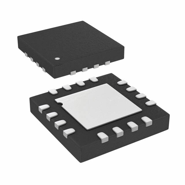
- Part No.:
- ADL5317ACPZ-REEL7
- Manufacturer:
- Analog Devices Inc.
- Category:
- Current Regulation/Management
- Package:
- 16-VFQFN Exposed Pad, CSP
- Datasheet:
-
 ADL5317ACPZ-REEL7.pdf
- Description:
- IC CURRENT MONITOR 16LFCSP
- Quantity:
- Payment:

- Shipping:

Inventory:1,681
Please send an inquiry. Send us your inquiry, and we will respond immediately.
Product details
Overview
ADL5317ACPZ-REEL7 from Analog Devices is a high-voltage avalanche photodiode (APD) bias controller and wide-range current monitor IC. It delivers precise 6 V to 75 V APD bias voltage via 3 V-compatible VSET input, mirrors photodiode current (IAPD) with 5:1 attenuation to IPDM output, achieves 0.25% linearity from 10 nA to 1 mA, and integrates overcurrent/overtemperature protection. It is used in fiber-optic receivers for stable optical power monitoring and APD biasing under temperature and signal variation.
For engineers reviewing the ADL5317ACPZ-REEL7 datasheet, ADL5317ACPZ-REEL7 pinout, ADL5317ACPZ-REEL7 application, or ADL5317ACPZ-REEL7 equivalent, this page provides verified functional identity, validated 16-lead LFCSP package mapping, confirmed 5:1 current mirror ratio and 30× VSET gain, real-world supply tracking mode behavior, and two technically documented alternative parts for APD bias control systems.
Technical Context
The ADL5317ACPZ-REEL7 implements a JFET-input amplifier driving a bipolar current mirror with proprietary cascoding to maintain 0.2% gain stability across −40°C to +85°C and 10 V–80 V VPHV supply range. Its VSET-to-VAPD transfer function is fixed at 29.7–30.3 V/V with <0.5 mV offset, while the IPDM output delivers 0.198–0.202 A/A current gain independent of VAPD voltage.
It supports dual operating modes: linear mode (VSET = 0.2–2.5 V → VAPD = 30×VSET) and supply tracking mode (VSET = 3.0–5.5 V, VCLH open → VAPD = VPHV − 2.0 V). Protection includes 14–21 mA VAPD current compliance limit and thermal shutdown at 140°C with 20°C hysteresis, signaled via open-collector FALT pin.
Key Specifications
| Parameter | Value and Actual Design Meaning |
|---|---|
| VAPD Bias Range | 6 V to 75 V - sets APD reverse bias across full avalanche multiplication range without external components. |
| Current Monitor Ratio | 5:1 (IAPD/IPDM) - enables low-power, high-accuracy optical power measurement using logarithmic amplifiers. |
| Linearity Error | ±0.25% (10 nA–1 mA), ±0.5% (5 nA–5 mA) - ensures calibrated optical power readout over six decades. |
| VSET Input Gain | 29.7–30.3 V/V - allows direct 0.2–2.5 V DAC or sensor output to set precise APD bias voltage. |
| Supply Tracking Offset | 1.90–2.15 V below VPHV - maintains stable APD bias when paired with adjustable HV DC-DC converters. |
| Fault Detection | Open-collector FALT pin asserts low on >18 mA IAPD or >140°C die temperature - enables system-level fault handling. |
| Package | 16-lead LFCSP (3 mm × 3 mm) - compact footprint compatible with high-density optical module layouts. |
Pinout & Package
ADL5317ACPZ-REEL7 is housed in a 16-lead Lead Frame Chip Scale Package (LFCSP) with exposed paddle thermally and electrically connected to COMM. Pin 1 (FALT) is top-left corner; pins numbered counterclockwise. Exposed paddle must be soldered to ground plane via low-impedance path per datasheet Figure 2.
| Pin/Terminal | Circuit Role | Design Meaning |
|---|---|---|
| FALT (Pin 1) | Open-collector fault indicator | Asserts logic low during overcurrent (>18 mA) or overtemperature (>140°C); requires external pull-up ≤1 mA. |
| VSET (Pin 2) | Bias control voltage input | 0.2–2.5 V sets VAPD = 30×VSET in linear mode; 3.0–5.5 V enables supply tracking mode. |
| VPLV (Pin 3) | Low-voltage supply rail | 4–6 V powers internal logic and reference circuits; supplies quiescent current of 0.7–0.84 mA. |
| VPHV (Pins 4,5) | High-voltage supply input | 10–80 V powers APD bias circuitry; total quiescent draw rises to 4.5 mA at 1 mA IAPD. |
| VCLH (Pin 6) | VSET amplifier clamp control | Short to VPHV extends linear VAPD range; open enables supply tracking mode (VAPD = VPHV − 2.0 V). |
| GARD (Pins 7,9) | VAPD guard/shield driver | Tracks VAPD potential to reduce leakage and noise; requires external CGRD capacitor (up to 0.01 µF) to COMM. |
| VAPD (Pin 8) | APD bias output / current input | Sources up to 5 mA to APD cathode; voltage accuracy maintained across full IAPD range and temperature. |
| IPDM (Pin 11) | Monitored current output | Sources IAPD/5 (e.g., 1 µA IPDM = 5 µA IAPD); output compliance limited to min(VPLV, VAPD/3). |
| COMM (Pins 13–16) | Analog ground reference | All analog signals referenced to this node; exposed paddle must connect directly to COMM ground plane. |
Key Features
| Feature | Design Value |
|---|---|
| Integrated APD bias control + current monitor | Eliminates discrete op-amp, transistor, and resistor networks required for precision APD biasing and optical power feedback. |
| 6-decade current monitoring (5 nA–5 mA) | Enables single-device optical power measurement from ultra-low-light sensing to high-power burst-mode detection. |
| Supply tracking mode (VAPD = VPHV − 2.0 V) | Allows direct use with programmable HV supplies without recalibration; maintains 2.0 V headroom for APD breakdown margin. |
| On-chip overcurrent and thermal protection | Prevents APD damage during fault conditions; FALT pin provides fail-safe interface to host microcontroller or FPGA. |
| GARD-driven noise filtering | External CGRD capacitor reduces VSET amplifier noise contribution, enabling sub-nA level measurement fidelity. |
Applications
| Fiber-Optic Receiver Bias Control | Optical Power Monitoring in PON Systems |
|---|---|
Use Scenario: Stabilizing APD bias in GPON/EPON ONU receivers where ambient temperature varies from −40°C to +85°C and optical input power spans 30 dB. IC Role / Device Role / Timing Role: ADL5317ACPZ-REEL7 acts as closed-loop APD bias controller, adjusting VAPD in real time to maintain constant avalanche gain despite temperature drift. Use Value: Enables <±0.5% gain stability over temperature using only a DAC and temperature sensor-no manual calibration or trimming required. |
Use Scenario: Measuring received optical power in passive optical network splitters to dynamically adjust transmitter power and avoid upstream interference. IC Role / Device Role / Timing Role: ADL5317ACPZ-REEL7 serves as front-end current monitor, feeding IPDM output to AD8305 logarithmic amplifier for 60 dB dynamic range RSSI generation. Use Value: Delivers ±0.25% linearity from 10 nA to 1 mA, allowing accurate optical power reporting across all ONT operational states including sleep mode. |
| Laser Safety Interlock Circuit | LiDAR APD Signal Conditioning |
Use Scenario: Detecting hazardous optical power levels in Class 4 laser systems by monitoring APD current during alignment and operation. IC Role / Device Role / Timing Role: ADL5317ACPZ-REEL7 functions as safety-critical current monitor, asserting FALT within microseconds upon IAPD exceeding 18 mA threshold. Use Value: Provides hardware-level fault response independent of firmware, meeting IEC 60825-1 interlock timing requirements (<100 µs reaction). |
Use Scenario: Conditioning weak return pulses in short-pulse LiDAR, where APD current ranges from 1 nA (long range) to 5 mA (near object) at 100 kHz repetition rate. IC Role / Device Role / Timing Role: ADL5317ACPZ-REEL7 operates in linear mode to deliver fast VAPD settling (<20 µs) and preserves pulse fidelity via 2 MHz small-signal bandwidth at 5 µA IAPD. Use Value: Maintains <1% pulse amplitude error across full current range, enabling centimeter-level distance resolution without post-processing correction. |
Equivalent & Alternatives
The following parts are listed as comparable options for similar APD bias control and current monitoring applications.
| Alternative Part | Technical Difference | Application Difference | Selection Advice |
|---|---|---|---|
| MAX32682ETE+ | Lower VAPD range (0–36 V), integrated 12-bit DAC, no supply tracking mode, 10 nA–10 mA monitoring range. | Targeted at battery-powered portable optical sensors; lacks high-voltage capability for telecom APDs. | Select when system uses <40 V HV supply and requires on-chip DAC control; not suitable for 75 V APD biasing. |
| LT3482ES6#TRPBF | Dedicated APD bias controller only (no current monitor), 30–75 V output, external feedback resistors required for setpoint. | Used where optical power monitoring is handled separately (e.g., transimpedance amp + ADC); higher layout complexity. | Select when bias control is primary need and current monitoring is implemented externally; adds BOM cost and calibration overhead. |
Compared with MAX32682ETE+ and LT3482ES6#TRPBF, ADL5317ACPZ-REEL7 uniquely combines 75 V bias capability, 5:1 precision current mirroring, and supply tracking mode in a single 3 mm × 3 mm package-reducing component count by ≥40% and eliminating external gain-setting resistors in telecom and LiDAR designs.
Availability
ADL5317ACPZ-REEL7 is available at Aetrix Electronics and suitable for fiber-optic receiver design, PON optical power monitoring, laser safety interlocks, and LiDAR APD signal conditioning requiring stable component supply across extended temperature and high-voltage operating conditions.
Supply support for ADL5317ACPZ-REEL7 includes scheduled delivery planning, volume procurement assistance, BOM continuity management, traceable sourcing, and lifecycle availability coordination for OEM customers, industrial embedded developers, connected-device designers, and electronics production programs.
Manufacturer
Analog Devices, Inc. is a global semiconductor leader specializing in high-performance analog, mixed-signal, and digital signal processing technologies for precision measurement and control systems.
The ADL5317ACPZ-REEL7 belongs to Analog Devices' optical interface product line, engineered specifically for avalanche photodiode biasing and wide-dynamic-range optical power monitoring in telecom, industrial sensing, and defense applications.
FAQ
What is the maximum VPHV supply voltage supported by the ADL5317ACPZ-REEL7?
The ADL5317ACPZ-REEL7 supports a maximum high-voltage supply (VPHV) of 80 V, as specified in Absolute Maximum Ratings. Operation at 78 V is validated in typical performance characteristics, and the device maintains full functionality-including 75 V VAPD output and 5:1 current mirroring-up to this limit. Exceeding 80 V risks permanent damage per Table 2.
Can the ADL5317ACPZ-REEL7 operate without an external CGRD capacitor on the GARD pin?
No, the ADL5317ACPZ-REEL7 requires an external capacitor (CGRD) from GARD to COMM for stable operation. The GARD pin drives a 20 kΩ internal resistor forming a low-pass filter; without CGRD, VSET amplifier noise couples directly into VAPD, degrading linearity and increasing output noise. Datasheet Figure 20 and Theory of Operation section mandate CGRD placement for all operating conditions.
How does the ADL5317ACPZ-REEL7 handle overtemperature events, and what happens to VAPD during shutdown?
When die temperature exceeds 140°C, the ADL5317ACPZ-REEL7 shuts down the current mirror and bias controller, pulling VAPD toward ground and asserting FALT low. The device remains latched off until temperature falls below 120°C (140°C − 20°C hysteresis), then automatically recovers. During shutdown, no current is sourced from VAPD, protecting the connected APD from thermal runaway.
Is the ADL5317ACPZ-REEL7 pin-compatible with earlier revisions like ADL5317ACPZ?
Yes, ADL5317ACPZ-REEL7 is a tape-and-reel packaging variant of the same die and package as ADL5317ACPZ. Both share identical pinout, electrical specifications, and thermal characteristics per Rev. A datasheet ordering guide. The "-REEL7" suffix denotes 7-inch reel packaging; no functional or mechanical differences exist between the two orderable part numbers.
What is the minimum IAPD current that can be accurately monitored by the ADL5317ACPZ-REEL7?
The ADL5317ACPZ-REEL7 guarantees ±0.5% linearity down to 5 nA IAPD, with typical performance showing ±0.25% error from 10 nA to 1 mA. At 5 nA, IPDM output is 1 nA (5 nA ÷ 5), and datasheet Figure 3 confirms measurable linearity across this point. For optimal low-current accuracy, CGRD ≥ 2 nF and proper guarding of VAPD/GARD traces are required.
ADL5317ACPZ-REEL7 Specifications
- Product attributes
- Attribute value
- Manufacturer:
- Analog Devices Inc.
- Series:
- -
- Package/Case:
- 16-VFQFN Exposed Pad, CSP
- Packaging:
- Tape & Reel (TR)
- Product Status:
- Active
- Function:
- Current Monitor
- Sensing Method:
- High-Side
- Accuracy:
- -
- Voltage - Input:
- 10V ~ 80V
- Current - Output:
- -
- Operating Temperature:
- -40°C ~ 85°C
- Grade:
- -
- Qualification:
- -
- Mounting Type:
- Surface Mount
- Supplier Device Package:
- 16-LFCSP-VQ (3x3)
ADL5317ACPZ-REEL7 FAQ
1.How can I place an order for ADL5317ACPZ-REEL7 through Aetrix?
Please submit a Request for Quotation (RFQ) for ADL5317ACPZ-REEL7 on Aetrix. Our sales agent will provide a competitive quotation and guide you through the order confirmation once you accept the terms.
2.Are the price and stock information for ADL5317ACPZ-REEL7 reliable?
The price and inventory of ADL5317ACPZ-REEL7 are updated periodically and may fluctuate due to market conditions. Stock and pricing data are typically refreshed every 24 hours. Quotation validity for ADL5317ACPZ-REEL7 is usually 5 days.
3.What payment methods are accepted for ADL5317ACPZ-REEL7?
We accept Wire Transfer, PayPal, Credit Card, Western Union, MoneyGram, and Escrow for ADL5317ACPZ-REEL7 transactions.
Note: Certain payment methods may incur a processing fee.
4.How is shipping managed for ADL5317ACPZ-REEL7?
ADL5317ACPZ-REEL7 orders can be shipped via leading logistics carriers, including DHL, UPS, FedEx, TNT, or Registered Mail.
Once your ADL5317ACPZ-REEL7 order is processed, you will receive an email with the shipment details and tracking number.
Note: Tracking information may take up to 24 hours to appear. Express delivery typically takes 3–5 business days.
5.How can I obtain technical support or documentation for ADL5317ACPZ-REEL7?
For technical support, including ADL5317ACPZ-REEL7 datasheets, pinout diagrams, or application guidance, please contact our engineering support team. They can provide detailed documentation and assistance for your ADL5317ACPZ-REEL7 requirements.
6.How does Aetrix verify that ADL5317ACPZ-REEL7 is sourced from the original manufacturer or authorized distributors?
All ADL5317ACPZ-REEL7 products on Aetrix are procured from qualified distributors and authorized channels. Our dedicated quality assurance team conducts strict verification, including traceability checks and, if necessary, third-party testing. This ensures that ADL5317ACPZ-REEL7 meets industry standards.
7.What is the process for return or replacement of ADL5317ACPZ-REEL7?
All ADL5317ACPZ-REEL7 units undergo pre-shipment inspection (PSI). If there is an issue with ADL5317ACPZ-REEL7, returns or replacements are accepted under the following conditions:
1.Quantity discrepancies, incorrect items, or visible external defects (such as breakage or corrosion), acknowledged by Aetrix.
2.The issue is reported within 90 days of delivery.
3.The ADL5317ACPZ-REEL7 part is unused and in its original packaging.
Return procedure for ADL5317ACPZ-REEL7:
1.Submit a request within 90 days.
2.Obtain a Return Material Authorization (RMA) from Aetrix.
ADL5317ACPZ-REEL7 Tags
.jpg)
-
PSSI2021SAY,115
Nexperia USA Inc.

-
BCR401RE6327HTSA1
Infineon Technologies

-
INA199B2DCKR
Texas Instruments
-
INA199A1DCKR
Texas Instruments
-
INA199B1DCKR
Texas Instruments
-
NSI45015WT1G
onsemi
-
NSI45020T1G
onsemi
-
NSI45030AT1G
onsemi
-
NSI45025AT1G
onsemi
-
NSI45020AT1G
onsemi
-
NSI50010YT1G
onsemi
-
LM334Z/NOPB
Texas Instruments
Tech Hub

A practical engineering guide to 3.3V and 5V logic compatibility, input thresholds, resistor dividers, translator ICs, MOSFET level shifting, I2C pull-ups, timing limits and power-sequencing risks.

The 74HC595 uses push-pull logic outputs, while the TPIC6B595 uses 50 V open-drain DMOS sinks for higher-power loads. This guide compares timing, current limits, 3.3 V interfacing, load wiring, thermal…

The 74HC595 converts serial data into eight stable parallel outputs. This guide covers pin functions, shift and storage timing, OE and MR behavior, drive-current limits, cascading, voltage compatibilit…

A technical comparison of level-sensitive latches and edge-triggered flip-flops, covering timing windows, setup and hold limits, master–slave operation, time borrowing, race-through, HDL inference and…

A D latch stores one bit while Enable controls when data can pass. This reference covers gate-level operation, truth tables, transparency, setup and hold timing, LE versus OE, common ICs and practical …

An SR latch stores one bit through cross-coupled feedback. This engineering reference covers NOR and NAND implementations, truth tables, forbidden-state recovery, gated operation, switch debouncing, fa…

Latch circuits retain one bit through feedback. This technical reference covers SR and D latches, truth tables, transparency, timing limits, latch-versus-flip-flop behavior, applications and common log…

An engineering guide to LED driver operation, constant-current and constant-voltage outputs, linear and switching topologies, dimming, IC selection, calculations, replacement compatibility, and fault c…

Operational amplifier guide covering op amp basics, feedback, ideal vs real op amps, common configurations, buffer circuits, offset, bias current, gain-bandwidth, slew rate, rail-to-rail limits and sel…

Jumper cables guide covering safe connection order, red and black clamp placement, final ground connection, cable gauge, length, clamp quality, copper vs CCA cables, jump starter comparison and battery…


