
 My Inquiry
 My Account


Analog Devices Inc. ADM1064ASU
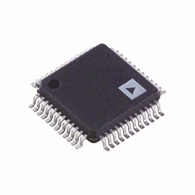
- Part No.:
- ADM1064ASU
- Manufacturer:
- Analog Devices Inc.
- Category:
- Supervisors
- Package:
- 48-TQFP
- Datasheet:
-
 ADM1064ASU.pdf
- Description:
- IC SUPERVISOR/SEQUENCER 48-TQFP
- Quantity:
- Payment:

- Shipping:

Inventory:249
Please send an inquiry. Send us your inquiry, and we will respond immediately.
Product details
Overview
ADM1064ASU from Analog Devices is a configurable supervisory and sequencing IC for multivoltage systems, integrating 10 supply fault detectors (±1% accuracy across −40°C to +85°C), a 12-bit SAR ADC for voltage readback of up to 12 channels, and 10 programmable driver outputs (PDOs) with dual-mode operation (LV logic or HV FET gate drive). It enables precise power-up/down sequencing in DSP/FPGA boards and telecom line cards.
For engineers reviewing the ADM1064ASU datasheet, ADM1064ASU pinout, ADM1064ASU application, or ADM1064ASU equivalent, key selection considerations include its 40-lead LFCSP package, SMBus programmability, 12 V charge-pumped PDO output capability (PDO1–PDO6), 0.573 V to 14.4 V supervision range, and integrated EEPROM for configuration persistence.
Technical Context
The ADM1064ASU implements a state-machine-based Sequencing Engine (SE) supporting up to 63 programmable states, enabling conditional transitions based on input events (e.g., supply OK, fault detection, watchdog timeout). Its architecture decouples supervision logic from sequencing control via dedicated SFDs and configurable PDO drivers.
Power is autonomously arbitrated among VH (up to 14.4 V) and VPx (up to 6.0 V) inputs, generating a regulated 4.75 V VDDCAP supply with <0.2 V dropout. The 12-bit ADC uses an internal 2.048 V reference (REFOUT) or external REFIN, with round-robin scanning across VH, VP1–VP4, VX1–VX5, AUX1, AUX2, and REFIN.
Key Specifications
| Parameter | Value and Actual Design Meaning |
|---|---|
| Supply Supervision Accuracy | ±1% over −40°C to +85°C - ensures reliable fault detection across industrial temperature range without calibration drift. |
| ADC Resolution & Range | 12-bit SAR, 0 to VREFIN - supports precise readback of all supervised supplies and aux inputs with ±2.5 LSB INL. |
| PDO Output Modes | 6 HV outputs (11–14 V, charge-pumped) + 10 LV outputs (VDDCAP/VPx referenced) - enables direct N-FET gate driving or logic-level enable signals. |
| Input Voltage Ranges | VH: 2.5–14.4 V; VPx: 0.573–6.0 V; VXx: 0.573–1.375 V - covers core, I/O, and auxiliary rails in modern multivoltage systems. |
| SMBus Interface | 400 kHz compliant - allows real-time configuration updates, fault reporting, and voltage monitoring without host CPU overhead. |
| Package | 40-lead LFCSP (6 mm × 6 mm, exposed pad) - provides low thermal resistance (θJA = 25°C/W) for high-density board layouts. |
| User EEPROM | 256 bytes - stores full device configuration (SFD thresholds, SE states, PDO mappings) for autonomous operation at power-up. |
Pinout & Package
ADM1064ASU is housed in a 40-lead LFCSP (Lead Frame Chip Scale Package) with 6 mm × 6 mm footprint and exposed thermal pad (NC, soldered for mechanical stability only).
| Pin/Terminal | Circuit Role | Design Meaning |
|---|---|---|
| VH (Pin 10) | High-voltage supply input & fault detector | Accepts 3.0–14.4 V; powers VDDCAP when highest active rail; enables supervision of 12 V backplanes. |
| VP1–VP4 (Pins 6–9) | Low-voltage supply inputs & fault detectors | Each supports 3 ranges (ultralow/mid/low); supervise 1.25–6.0 V rails like core voltages or I/O supplies. |
| VX1–VX5 (Pins 1–5) | Dual-function analog/digital inputs | Configurable as SFDs (0.573–1.375 V) or CMOS/TTL logic inputs - adds flexibility for margin testing or GPIO. |
| PDO1–PDO6 (Pins 30–25) | Charge-pumped high-voltage outputs | Drive N-FET gates up to 14 V with 20 μA average current - eliminates need for external level shifters. |
| PDO7–PDO10 (Pins 24–21) | LV programmable outputs | Push-pull or open-collector (weak pull-up to VDDCAP/VPx) - suitable for enabling DC/DC converters or reset signals. |
| SDA/SCL (Pins 36/35) | SMBus bidirectional interface | Open-drain pins requiring external pull-ups; support standard 400 kHz protocol for configuration and monitoring. |
| VDDCAP (Pin 39) | Regulated internal supply output | 4.75 V LDO output derived from VH/VPx; powers internal circuitry and serves as pull-up source for PDO7–PDO10. |
| REFOUT/REFIN (Pins 14/13) | On-chip reference generator & ADC reference input | 2.048 V ±0.25% REFOUT drives REFIN; enables accurate ADC conversions without external reference. |
Key Features
| Feature | Design Value |
|---|---|
| 10-channel supply supervision | Supports undervoltage, overvoltage, and out-of-window fault detection on up to 10 rails with 8-bit threshold resolution. |
| State-machine Sequencing Engine | 63-state programmable engine enables complex, event-driven power sequencing (e.g., staggered ramp-up, fault recovery paths). |
| Integrated 12-bit ADC | Reads back VH, VP1–VP4, VX1–VX5, AUX1, AUX2, and REFIN - enables closed-loop margining and real-time telemetry. |
| Configurable PDO drivers | 6 HV outputs (charge-pumped) + 4 additional LV outputs - simplifies board design by replacing discrete FET drivers and logic buffers. |
| Autonomous power arbitration | VDDCAP sourced from highest of VH or VPx (≥3.0 V), ensuring operation during partial supply loss - critical for telecom redundancy. |
| User EEPROM storage | 256-byte nonvolatile memory retains full configuration (SFD settings, SE states, PDO modes) across power cycles. |
Applications
| Telecom Line Cards | Server Power Subsystems |
|---|---|
Use Scenario: Monitoring and sequencing multiple voltage rails (12 V backplane, 3.3 V, 1.8 V, 1.2 V) on carrier-grade line cards with hot-swap capability. IC Role / Device Role / Timing Role: Central supervisory sequencer coordinating power delivery to ASICs, FPGAs, and transceivers while detecting brownouts. Use Value: Prevents system lockup during partial supply failure by triggering controlled shutdown via PDO-driven enable/disable signals. |
Use Scenario: Managing power-up sequence of CPU core, memory, and I/O rails in dual-socket server motherboards with strict timing requirements. IC Role / Device Role / Timing Role: Timing-critical sequencer enforcing millisecond-accurate delays between rail activations using internal oscillator (100 kHz). Use Value: Eliminates need for external RC timers or CPLDs, reducing BOM count and layout complexity. |
| FPGA/ASIC Development Boards | In-Circuit Supply Margining |
Use Scenario: Providing flexible, reprogrammable sequencing for prototype FPGA platforms with varying core/I/O voltage combinations. IC Role / Device Role / Timing Role: Configurable supervisor adapting to different FPGA families (Xilinx Versal, Intel Agilex) via SMBus-hosted GUI tool. Use Value: Enables rapid iteration of power sequences without hardware changes - accelerates bring-up and validation. |
Use Scenario: Performing automated in-circuit voltage margining tests by reading back actual rail values via ADC and adjusting supplies dynamically. IC Role / Device Role / Timing Role: Precision ADC front-end with 12-bit resolution and 0.25 LSB rms noise - captures small deviations during stress testing. Use Value: Replaces external DMMs for rail verification, enabling real-time pass/fail decisions in production test fixtures. |
Equivalent & Alternatives
The following parts are listed as comparable options for similar multirail supervisory sequencing applications.
| Alternative Part | Technical Difference | Application Difference | Selection Advice |
|---|---|---|---|
| ADM1168ACPZ | 8-channel supervision, no integrated ADC, 6 PDOs with 12 V drive, same 40-lead LFCSP package | Lacks voltage readback capability - requires external ADC or monitoring IC for telemetry | Select when sequencing-only functionality suffices and ADC telemetry is handled elsewhere. |
| TPS40422RTWR | 2-channel PMBus sequencer with 12-bit ADC, 4 programmable outputs, 24-pin QFN, no charge-pump HV drive | Lower channel count and no >6 V PDO output - unsuitable for 12 V FET gate driving | Choose for compact, dual-rail applications where space is constrained and HV drive is unnecessary. |
Compared with ADM1064ASU, ADM1168ACPZ offers identical packaging and HV PDO capability but omits ADC-based telemetry, while TPS40422RTWR provides PMBus compatibility and smaller footprint but lacks the 12 V charge-pumped outputs needed for direct N-FET control - making ADM1064ASU uniquely suited for high-voltage sequencing with integrated diagnostics.
Availability
ADM1064ASU is available at Aetrix Electronics and suitable for telecom line cards, server power subsystems, FPGA development platforms, and in-circuit margining test fixtures requiring stable component supply, long-term lifecycle support, and guaranteed traceable sourcing.
Supply support for ADM1064ASU includes scheduled delivery planning, volume procurement assistance, BOM continuity management, traceable sourcing, and lifecycle availability coordination for OEM customers, industrial embedded developers, connected-device designers, and electronics production programs.
Manufacturer
Analog Devices, Inc. is a global leader in high-performance analog, mixed-signal, and digital signal processing semiconductors, headquartered in Norwood, MA, with design centers worldwide.
The ADM1064ASU belongs to Analog Devices' Super Sequencer® family, engineered specifically for robust, software-configurable power supervision and sequencing in multivoltage infrastructure equipment where reliability, precision, and integration are critical.
FAQ
What is the primary function of the ADM1064ASU in a power system?
The ADM1064ASU serves as a fully configurable supervisory sequencer that monitors up to 10 voltage rails with ±1% accuracy, executes programmable power-up/down sequences via its 63-state Sequencing Engine, and provides 12-bit ADC-based voltage readback. In systems like telecom line cards, the ADM1064ASU replaces discrete supervisors and timers, centralizing control while enabling real-time telemetry and fault response - all within a single 40-lead LFCSP package.
How does the ADM1064ASU handle power supply redundancy?
The ADM1064ASU implements autonomous power arbitration among VH (up to 14.4 V) and VP1–VP4 (up to 6.0 V) inputs, selecting the highest valid supply ≥3.0 V to generate its internal 4.75 V VDDCAP rail. This architecture ensures continuous operation during partial supply loss - for example, if the 12 V backplane fails, the device seamlessly switches to a 3.3 V auxiliary rail. The ADM1064ASU's VDDCAP remains stable even during transient brownouts, thanks to an external 10 μF reservoir capacitor.
Can the ADM1064ASU drive N-channel MOSFETs directly?
Yes - six of the ADM1064ASU's programmable driver outputs (PDO1–PDO6) feature an internal charge pump that delivers 11–14 V at up to 20 μA average current, sufficient to fully enhance common N-channel power FETs used in high-side switching applications. This eliminates external level-shifting circuitry. The remaining four PDOs (PDO7–PDO10) operate in LV mode, providing push-pull or weak pull-up outputs referenced to VDDCAP or VPx - ideal for enabling DC/DC converters or asserting reset signals.
What interfaces does the ADM1064ASU support for configuration and monitoring?
The ADM1064ASU uses a standard 400 kHz SMBus 2-wire interface (SDA/SCL pins) for full read/write access to all registers, including supply thresholds, sequencing states, PDO configurations, and ADC results. Configuration data is stored in 256 bytes of on-chip EEPROM, enabling autonomous operation at power-up without host intervention. Analog Devices provides a GUI-based configuration tool that communicates with the ADM1064ASU over SMBus to simplify setup and validation of complex sequencing logic.
Does the ADM1064ASU require an external voltage reference for ADC operation?
No - the ADM1064ASU integrates a precision 2.048 V ±0.25% reference (REFOUT) that can be directly connected to its REFIN pin to serve as the ADC reference. This eliminates the need for an external reference and ensures consistent 12-bit conversion accuracy across temperature. Alternatively, a higher-accuracy external reference may be applied to REFIN for improved ADC performance in metrology-grade applications, but the internal REFOUT is sufficient for typical power-supply monitoring tasks.
ADM1064ASU Specifications
- Product attributes
- Attribute value
- Manufacturer:
- Analog Devices Inc.
- Series:
- -
- Package/Case:
- 48-TQFP
- Packaging:
- Bag
- Product Status:
- Obsolete
- Programmable:
- Not Verified
- Type:
- Sequencer
- Number of Voltages Monitored:
- 10
- Voltage - Threshold:
- Adjustable/Selectable
- Output:
- Programmable
- Reset:
- -
- Reset Timeout:
- -
- Operating Temperature:
- -40°C ~ 85°C
- Grade:
- -
- Qualification:
- -
- Mounting Type:
- Surface Mount
- Supplier Device Package:
- 48-TQFP (7x7)
ADM1064ASU FAQ
1.How can I place an order for ADM1064ASU through Aetrix?
Please submit a Request for Quotation (RFQ) for ADM1064ASU on Aetrix. Our sales agent will provide a competitive quotation and guide you through the order confirmation once you accept the terms.
2.Are the price and stock information for ADM1064ASU reliable?
The price and inventory of ADM1064ASU are updated periodically and may fluctuate due to market conditions. Stock and pricing data are typically refreshed every 24 hours. Quotation validity for ADM1064ASU is usually 5 days.
3.What payment methods are accepted for ADM1064ASU?
We accept Wire Transfer, PayPal, Credit Card, Western Union, MoneyGram, and Escrow for ADM1064ASU transactions.
Note: Certain payment methods may incur a processing fee.
4.How is shipping managed for ADM1064ASU?
ADM1064ASU orders can be shipped via leading logistics carriers, including DHL, UPS, FedEx, TNT, or Registered Mail.
Once your ADM1064ASU order is processed, you will receive an email with the shipment details and tracking number.
Note: Tracking information may take up to 24 hours to appear. Express delivery typically takes 3–5 business days.
5.How can I obtain technical support or documentation for ADM1064ASU?
For technical support, including ADM1064ASU datasheets, pinout diagrams, or application guidance, please contact our engineering support team. They can provide detailed documentation and assistance for your ADM1064ASU requirements.
6.How does Aetrix verify that ADM1064ASU is sourced from the original manufacturer or authorized distributors?
All ADM1064ASU products on Aetrix are procured from qualified distributors and authorized channels. Our dedicated quality assurance team conducts strict verification, including traceability checks and, if necessary, third-party testing. This ensures that ADM1064ASU meets industry standards.
7.What is the process for return or replacement of ADM1064ASU?
All ADM1064ASU units undergo pre-shipment inspection (PSI). If there is an issue with ADM1064ASU, returns or replacements are accepted under the following conditions:
1.Quantity discrepancies, incorrect items, or visible external defects (such as breakage or corrosion), acknowledged by Aetrix.
2.The issue is reported within 90 days of delivery.
3.The ADM1064ASU part is unused and in its original packaging.
Return procedure for ADM1064ASU:
1.Submit a request within 90 days.
2.Obtain a Return Material Authorization (RMA) from Aetrix.
ADM1064ASU Tags
-
MIC826SYMT-TR
Microchip Technology

-
APX803S-31SA-7
Diodes Incorporated
-
APX803L20-29SA-7
Diodes Incorporated

-
TPS3828-33DBVR
Texas Instruments

-
V6340RSP3B+
EM Microelectronic
-
EM6325CXSP5B-2.9+
EM Microelectronic
-
MCP120T-300I/TT
Microchip Technology
-
MCP130T-315I/TT
Microchip Technology
-
MCP120T-475I/TT
Microchip Technology
-
MCP111T-300E/TT
Microchip Technology
-
MCP120T-315I/TT
Microchip Technology
-
MCP809T-315I/TT
Microchip Technology
Tech Hub

A practical engineering guide to 3.3V and 5V logic compatibility, input thresholds, resistor dividers, translator ICs, MOSFET level shifting, I2C pull-ups, timing limits and power-sequencing risks.

The 74HC595 uses push-pull logic outputs, while the TPIC6B595 uses 50 V open-drain DMOS sinks for higher-power loads. This guide compares timing, current limits, 3.3 V interfacing, load wiring, thermal…

The 74HC595 converts serial data into eight stable parallel outputs. This guide covers pin functions, shift and storage timing, OE and MR behavior, drive-current limits, cascading, voltage compatibilit…

A technical comparison of level-sensitive latches and edge-triggered flip-flops, covering timing windows, setup and hold limits, master–slave operation, time borrowing, race-through, HDL inference and…

A D latch stores one bit while Enable controls when data can pass. This reference covers gate-level operation, truth tables, transparency, setup and hold timing, LE versus OE, common ICs and practical …

An SR latch stores one bit through cross-coupled feedback. This engineering reference covers NOR and NAND implementations, truth tables, forbidden-state recovery, gated operation, switch debouncing, fa…

Latch circuits retain one bit through feedback. This technical reference covers SR and D latches, truth tables, transparency, timing limits, latch-versus-flip-flop behavior, applications and common log…

An engineering guide to LED driver operation, constant-current and constant-voltage outputs, linear and switching topologies, dimming, IC selection, calculations, replacement compatibility, and fault c…

Operational amplifier guide covering op amp basics, feedback, ideal vs real op amps, common configurations, buffer circuits, offset, bias current, gain-bandwidth, slew rate, rail-to-rail limits and sel…

Jumper cables guide covering safe connection order, red and black clamp placement, final ground connection, cable gauge, length, clamp quality, copper vs CCA cables, jump starter comparison and battery…


