
 My Inquiry
 My Account


Analog Devices Inc. ADM8693ARUZ
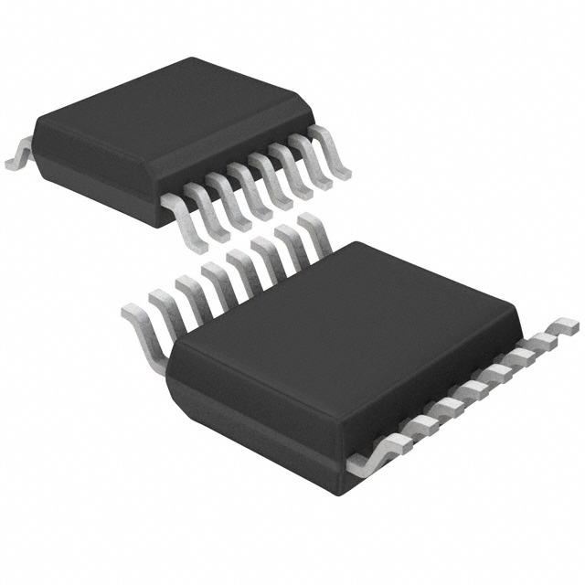
- Part No.:
- ADM8693ARUZ
- Manufacturer:
- Analog Devices Inc.
- Category:
- Supervisors
- Package:
- 16-TSSOP (0.173", 4.40mm Width)
- Datasheet:
-
 ADM8693ARUZ.pdf
- Description:
- IC SUPERVISOR 1 CHANNEL 16TSSOP
- Quantity:
- Payment:

- Shipping:

Inventory:1,516
Please send an inquiry. Send us your inquiry, and we will respond immediately.
Product details
Overview
ADM8693ARUZ from Analog Devices is a 16-lead TSSOP microprocessor supervisory circuit providing precision reset generation, adjustable watchdog timer (100 ms / 1.6 s / adjustable), battery backup switchover (VCC/VBATT to VOUT), power-fail warning (1.3 V PFI threshold), and CE signal gating with 3 ns propagation delay - all operating down to VCC = 1 V. It serves as a single-chip power integrity manager in industrial controllers and embedded systems requiring reliable brownout recovery and RAM write protection.
For engineers reviewing the ADM8693ARUZ datasheet, ADM8693ARUZ pinout, ADM8693ARUZ application, or ADM8693ARUZ equivalent, key selection criteria include its 4.40 V reset threshold, dual-mode watchdog timeout configurability, active-low RESET with guaranteed operation at 1 V, BATT ON output for external PNP drive, and CEIN/CEOUT gating for CMOS RAM write lockout during supply faults.
Technical Context
The ADM8693ARUZ integrates a precision voltage monitor (4.40 V ±50 mV hysteresis), a three-level WDI input with internal 38% VCC bias and ~5 MΩ impedance, and dual oscillator control (internal or external capacitor/clock) enabling independent adjustment of reset pulse width (50 ms or adjustable) and watchdog timeout. Its battery switchover uses asymmetric thresholds (70 mV rise, 50 mV fall) with 20 mV hysteresis to prevent chatter during slow VCC decay.
It features separate logic outputs: active-low RESET, active-high LOW LINE, open-drain WDO, push-pull BATT ON, and gated CEOUT - all synchronized to VCC validity. The PFI comparator (1.30 V ±25 mV) drives PFO low on undervoltage, while CEIN-to-CEOUT gating enforces write disable when VCC drops below 4.40 V, ensuring data integrity in battery-backed RAM.
Key Specifications
| Parameter | Value and Actual Design Meaning |
|---|---|
| Reset Threshold | 4.40 V (guaranteed 4.25–4.48 V); matches 5 V ±10% supplies and ensures robust brownout detection before microprocessor malfunction. |
| Reset Pulse Width | 50 ms typical (adjustable via OSC IN/OSC SEL); provides sufficient stabilization time for 8/16-bit MCUs after power-up or brownout recovery. |
| Watchdog Timeout | 100 ms short / 1.6 s long / adjustable; configurable via OSC SEL and OSC IN to support fast-recovery or safety-critical timing requirements. |
| VCC Operating Range | 4.5 V to 5.5 V; compatible with standard 5 V logic rails and tolerant of ±10% regulation tolerance. |
| Battery Backup Range | VBATT = 2.0 V to 4.0 V; supports common lithium, coin-cell, and supercapacitor backup sources without external regulation. |
| VOUT Drive Capability | 100 mA max (0.7 Ω on-resistance); directly powers CMOS RAM banks without external pass devices under normal operation. |
| Supply Current | 200 µA typical (active), 0.4 µA in battery backup; enables ultra-low-power retention in always-on embedded systems. |
Pinout & Package
ADM8693ARUZ is housed in a 16-lead TSSOP (RU-16) package with 0.65 mm pitch, optimized for high-density PCB layouts and industrial thermal performance (θJA = 158°C/W).
| Pin/Terminal | Circuit Role | Design Meaning |
|---|---|---|
| VCC | Primary power supply input | 5 V nominal rail; powers internal circuitry and feeds VOUT via low-RDS(on) PMOS switch (0.7 Ω). |
| VBATT | Backup battery input | Accepts 2.0–4.0 V sources; automatically selected by switchover logic when VCC falls below VBATT − 50 mV. |
| VOUT | Switched output rail | Delivers VCC or VBATT (whichever higher) to RAM; sustains 100 mA load with <0.2 V dropout at full current. |
| GND | Signal and power ground reference | Common 0 V return for all analog/digital functions; critical for accurate voltage threshold sensing. |
| RESET | Active-low reset output | Drives MCU reset pin low during power-up, brownout, or watchdog timeout; remains functional down to VCC = 1 V. |
| WDI | Watchdog input | Three-level input (biased to 38% VCC); toggling resets timer; floating or mid-supply disables watchdog. |
| PFI | Power-fail comparator input | Non-inverting input referenced to 1.30 V; triggers PFO low when supply-derived voltage drops below threshold. |
| PFO | Power-fail output | Active-low open-drain signal indicating imminent VCC collapse; used for early warning or controlled shutdown. |
| CEIN | Chip enable input | Logic input gated to CEOUT; must be driven low/high to enable/disable memory access during valid VCC. |
| CEOUT | Gated chip enable output | Replicates CEIN when VCC > 4.40 V; forced high during reset to block writes to battery-backed RAM. |
| BATT ON | Battery switchover status | Push-pull output high when VOUT sourced from VBATT; sinks 35 mA to drive external PNP base for >100 mA loads. |
| LOW LINE | Complementary reset indicator | Active-high inverse of RESET; useful for processors requiring active-high reset assertion. |
| OSC IN | Oscillator timing input | Accepts external clock (0–500 kHz) or 47 pF capacitor to set adjustable reset/watchdog timing. |
| OSC SEL | Oscillator mode select | High/floating = internal oscillator; low = external clock/capacitor mode; includes 3 µA internal pull-up. |
| WDO | Watchdog status output | Active-low open-drain flag that stays low after timeout until next WDI transition; aids debug and fault logging. |
Key Features
| Feature | Design Value |
|---|---|
| Adjustable reset & watchdog timing | Configurable via OSC SEL/OSC IN to support system-specific startup sequences and safety timeouts without firmware changes. |
| Guaranteed 1 V reset operation | Ensures microprocessor remains held in reset even during deep brownout or rapid VCC collapse, preventing undefined execution. |
| 3 ns CE gating propagation delay | Enables real-time write protection of battery-backed RAM with minimal impact on memory access timing in high-speed systems. |
| Asymmetric battery switchover thresholds | 70 mV turn-on / 50 mV turn-off hysteresis eliminates oscillation during slow VCC decay near VBATT voltage. |
| Integrated 1.3 V power-fail comparator | Provides deterministic early-warning signal (PFO) for controlled data save or state preservation before VCC failure. |
| Low 0.4 µA battery backup current | Extends coin-cell life to >10 years in standby, critical for unattended industrial logging and metering applications. |
Applications
| Industrial PLC Controller | Automotive Body Control Module |
|---|---|
Use Scenario: Power monitoring and safe shutdown during vehicle battery voltage sag or alternator failure. IC Role / Device Role / Timing Role: Supervisory circuit asserting RESET and disabling CEOUT to freeze RAM writes while triggering PFO-based log capture. Use Value: Prevents EEPROM corruption and preserves fault history across 12 V supply dips to 6 V, meeting ISO 16750-2 transient immunity requirements. |
Use Scenario: Maintaining real-time clock and configuration data during ignition-off battery drain. IC Role / Device Role / Timing Role: Battery switchover controller delivering stable 3.3 V-equivalent VOUT from 2.5 V LiMnO₂ cell while gating CEOUT to protect SRAM. Use Value: Enables >5-year backup runtime with 0.4 µA quiescent current and automatic write lockout during VCC dropout. |
| Medical Infusion Pump | Smart Energy Meter |
Use Scenario: Ensuring deterministic restart and data integrity after AC mains interruption or DC supply fault. IC Role / Device Role / Timing Role: Dual-role supervisor generating 200 ms RESET pulse (via OSC SEL config) and driving WDO for watchdog-triggered alarm escalation. Use Value: Meets IEC 62304 Class C software safety requirements via hardware-enforced reset timing and fail-safe state capture. |
Use Scenario: Preserving tariff data and metering registers during grid outage or tamper-induced power cut. IC Role / Device Role / Timing Role: Precision voltage monitor (4.40 V threshold) combined with PFI-driven PFO to initiate flash save before VCC drops below 4.25 V. Use Value: Guarantees zero data loss across 100,000+ power cycles using 4.40 V hysteresis and 50 mV switchover margin. |
Equivalent & Alternatives
The following parts are listed as comparable options for similar microprocessor supervisory applications.
| Alternative Part | Technical Difference | Application Difference | Selection Advice |
|---|---|---|---|
| ADM8691ARUZ | Same 16-lead TSSOP package and pinout; identical 4.65 V reset threshold and 100 ms/1.6 s watchdog options. | Targeted at 5 V ±5% systems (e.g., legacy industrial backplanes) rather than ±10% automotive/energy meter rails. | Select ADM8691ARUZ only if system VCC regulation is tighter and 4.65 V threshold better matches supply tolerance. |
| MAX693ESA+ | Maxim Integrated 8-pin SOIC; fixed 4.63 V reset threshold, no CE gating or adjustable timing; 20 µA supply current. | Lacks battery switchover, PFI/PFO, and CEIN/CEOUT - suitable only for basic reset-only applications. | Choose MAX693ESA+ only when board space is constrained and advanced supervision features are unnecessary. |
Compared with ADM8691ARUZ, ADM8693ARUZ offers lower reset threshold (4.40 V vs. 4.65 V) for wider 5 V supply tolerance coverage, while MAX693ESA+ omits battery management and memory protection entirely - making ADM8693ARUZ the sole choice for systems requiring integrated RAM write lockout and dual-rail switchover.
Availability
ADM8693ARUZ is available at Aetrix Electronics and suitable for industrial PLC controllers, automotive body control modules, medical infusion pumps, and smart energy meters requiring stable component supply with guaranteed long-term lifecycle support.
Supply support for ADM8693ARUZ includes scheduled delivery planning, volume procurement assistance, BOM continuity management, traceable sourcing, and lifecycle availability coordination for OEM customers, industrial embedded developers, connected-device designers, and electronics production programs.
Manufacturer
Analog Devices is a global leader in high-performance analog, mixed-signal, and digital signal processing semiconductors, serving industrial, automotive, communications, and healthcare markets since 1965.
The ADM869x family was designed specifically for microprocessor system integrity - integrating reset, watchdog, battery switchover, power-fail warning, and memory write protection into a single IC to eliminate discrete supervision complexity in space-constrained embedded designs.
FAQ
What is the guaranteed reset voltage threshold for ADM8693ARUZ?
The ADM8693ARUZ has a guaranteed reset voltage threshold of 4.25 V minimum to 4.48 V maximum, with a typical value of 4.40 V. This specification ensures reliable reset assertion across the full industrial temperature range (−40°C to +85°C) and matches 5 V ±10% power supplies. The 4.40 V threshold is factory-trimmed and tested per Analog Devices' Rev. B datasheet, Table 2.
Can ADM8693ARUZ operate with VCC as low as 1 V, and what does that mean for system reliability?
Yes, ADM8693ARUZ guarantees RESET output functionality down to VCC = 1 V, meaning it continues asserting reset to the microprocessor even during severe brownout or rapid power collapse. This prevents the MCU from executing random instructions or entering undefined states. The 1 V operation is validated per datasheet Figure 7 and ensures fail-safe shutdown in systems where backup capacitors sustain VCC just above 1 V for several milliseconds.
How does the battery switchover hysteresis work in ADM8693ARUZ, and why is it important?
ADM8693ARUZ uses asymmetric hysteresis: VOUT switches from VCC to VBATT when VCC falls to VBATT − 50 mV, and switches back when VCC rises to VBATT + 70 mV - yielding 20 mV total hysteresis. This prevents oscillatory switching during slow VCC decay near VBATT voltage, which could cause RAM corruption or logic glitches. The behavior is documented in the Battery Switchover Section (Page 10) and Figure 14 of the datasheet.
What are the exact pin functions of CEIN and CEOUT on ADM8693ARUZ, and how do they protect memory?
CEIN is the chip-enable input signal fed into the ADM8693ARUZ; CEOUT is its gated output. When VCC ≥ 4.40 V, CEOUT replicates CEIN with 3 ns delay. When VCC drops below threshold, CEOUT is forced high - disabling write access to battery-backed CMOS RAM. This hardware-enforced lockout prevents data corruption during power faults and is detailed in Figure 21 and the CE Gating section (Page 12) of the datasheet.
Is ADM8693ARUZ pin-compatible with other devices in the ADM869x family, and which ones share the same 16-lead TSSOP footprint?
Yes, ADM8693ARUZ is pin-compatible with ADM8691ARUZ and ADM8695ARUZ - all use the identical 16-lead TSSOP (RU-16) package and share identical pinout per Figure 4 and Table 4. Differences lie in reset threshold (4.40 V vs. 4.65 V vs. 4.65 V), reset timeout (50 ms vs. 50 ms vs. 200 ms), and watchdog configuration options - but PCB layout and interconnect remain unchanged across these variants.
ADM8693ARUZ Specifications
- Product attributes
- Attribute value
- Manufacturer:
- Analog Devices Inc.
- Series:
- -
- Package/Case:
- 16-TSSOP (0.173", 4.40mm Width)
- Packaging:
- Tube
- Product Status:
- Obsolete
- Programmable:
- Not Verified
- Type:
- Battery Backup Circuit
- Number of Voltages Monitored:
- 1
- Voltage - Threshold:
- 4.4V
- Output:
- Push-Pull, Push-Pull
- Reset:
- Active High/Active Low
- Reset Timeout:
- 35ms Minimum
- Operating Temperature:
- -40°C ~ 85°C (TA)
- Grade:
- -
- Qualification:
- -
- Mounting Type:
- Surface Mount
- Supplier Device Package:
- 16-TSSOP
ADM8693ARUZ FAQ
1.How can I place an order for ADM8693ARUZ through Aetrix?
Please submit a Request for Quotation (RFQ) for ADM8693ARUZ on Aetrix. Our sales agent will provide a competitive quotation and guide you through the order confirmation once you accept the terms.
2.Are the price and stock information for ADM8693ARUZ reliable?
The price and inventory of ADM8693ARUZ are updated periodically and may fluctuate due to market conditions. Stock and pricing data are typically refreshed every 24 hours. Quotation validity for ADM8693ARUZ is usually 5 days.
3.What payment methods are accepted for ADM8693ARUZ?
We accept Wire Transfer, PayPal, Credit Card, Western Union, MoneyGram, and Escrow for ADM8693ARUZ transactions.
Note: Certain payment methods may incur a processing fee.
4.How is shipping managed for ADM8693ARUZ?
ADM8693ARUZ orders can be shipped via leading logistics carriers, including DHL, UPS, FedEx, TNT, or Registered Mail.
Once your ADM8693ARUZ order is processed, you will receive an email with the shipment details and tracking number.
Note: Tracking information may take up to 24 hours to appear. Express delivery typically takes 3–5 business days.
5.How can I obtain technical support or documentation for ADM8693ARUZ?
For technical support, including ADM8693ARUZ datasheets, pinout diagrams, or application guidance, please contact our engineering support team. They can provide detailed documentation and assistance for your ADM8693ARUZ requirements.
6.How does Aetrix verify that ADM8693ARUZ is sourced from the original manufacturer or authorized distributors?
All ADM8693ARUZ products on Aetrix are procured from qualified distributors and authorized channels. Our dedicated quality assurance team conducts strict verification, including traceability checks and, if necessary, third-party testing. This ensures that ADM8693ARUZ meets industry standards.
7.What is the process for return or replacement of ADM8693ARUZ?
All ADM8693ARUZ units undergo pre-shipment inspection (PSI). If there is an issue with ADM8693ARUZ, returns or replacements are accepted under the following conditions:
1.Quantity discrepancies, incorrect items, or visible external defects (such as breakage or corrosion), acknowledged by Aetrix.
2.The issue is reported within 90 days of delivery.
3.The ADM8693ARUZ part is unused and in its original packaging.
Return procedure for ADM8693ARUZ:
1.Submit a request within 90 days.
2.Obtain a Return Material Authorization (RMA) from Aetrix.
ADM8693ARUZ Tags
-
MIC826SYMT-TR
Microchip Technology

-
APX803S-31SA-7
Diodes Incorporated
-
APX803L20-29SA-7
Diodes Incorporated

-
TPS3828-33DBVR
Texas Instruments

-
V6340RSP3B+
EM Microelectronic
-
EM6325CXSP5B-2.9+
EM Microelectronic
-
MCP120T-300I/TT
Microchip Technology
-
MCP130T-315I/TT
Microchip Technology
-
MCP120T-475I/TT
Microchip Technology
-
MCP111T-300E/TT
Microchip Technology
-
MCP120T-315I/TT
Microchip Technology
-
MCP809T-315I/TT
Microchip Technology
Tech Hub

A practical engineering guide to 3.3V and 5V logic compatibility, input thresholds, resistor dividers, translator ICs, MOSFET level shifting, I2C pull-ups, timing limits and power-sequencing risks.

The 74HC595 uses push-pull logic outputs, while the TPIC6B595 uses 50 V open-drain DMOS sinks for higher-power loads. This guide compares timing, current limits, 3.3 V interfacing, load wiring, thermal…

The 74HC595 converts serial data into eight stable parallel outputs. This guide covers pin functions, shift and storage timing, OE and MR behavior, drive-current limits, cascading, voltage compatibilit…

A technical comparison of level-sensitive latches and edge-triggered flip-flops, covering timing windows, setup and hold limits, master–slave operation, time borrowing, race-through, HDL inference and…

A D latch stores one bit while Enable controls when data can pass. This reference covers gate-level operation, truth tables, transparency, setup and hold timing, LE versus OE, common ICs and practical …

An SR latch stores one bit through cross-coupled feedback. This engineering reference covers NOR and NAND implementations, truth tables, forbidden-state recovery, gated operation, switch debouncing, fa…

Latch circuits retain one bit through feedback. This technical reference covers SR and D latches, truth tables, transparency, timing limits, latch-versus-flip-flop behavior, applications and common log…

An engineering guide to LED driver operation, constant-current and constant-voltage outputs, linear and switching topologies, dimming, IC selection, calculations, replacement compatibility, and fault c…

Operational amplifier guide covering op amp basics, feedback, ideal vs real op amps, common configurations, buffer circuits, offset, bias current, gain-bandwidth, slew rate, rail-to-rail limits and sel…

Jumper cables guide covering safe connection order, red and black clamp placement, final ground connection, cable gauge, length, clamp quality, copper vs CCA cables, jump starter comparison and battery…


