
 My Inquiry
 My Account


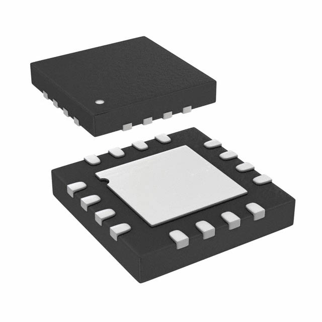
Analog Devices Inc. ADN2526ACPZ
- Part No.:
- ADN2526ACPZ
- Manufacturer:
- Analog Devices Inc.
- Category:
- Laser Drivers
- Package:
- 16-WFQFN Exposed Pad, CSP
- Datasheet:
-
 ADN2526ACPZ.pdf
- Description:
- IC LASER DRV 11.3GB 3.6V 16LFCSP
- Quantity:
- Payment:

- Shipping:

Inventory:2,107
Please send an inquiry. Send us your inquiry, and we will respond immediately.
Product details
Overview
ADN2526ACPZ from Analog Devices is a 11.3 Gbps differential laser diode driver with active back-termination, designed for direct modulation of TOSAs with 5 Ω–50 Ω differential resistance. It delivers 24 ps typical rise/fall times, 10–100 mA programmable bias current, and 10–80 mA differential modulation current, enabling high-fidelity optical eye generation in SFP+/XFP 10G transceivers.
For engineers reviewing the ADN2526ACPZ datasheet, ADN2526ACPZ pinout, ADN2526ACPZ application, or ADN2526ACPZ equivalent, key selection criteria include its SFP+ MSA compliance, ALS-controlled shutdown timing (2 µs assert / 10 µs negate), crosspoint adjustment capability, IBMON bias monitoring accuracy (±2% at 70–100 mA), and thermal performance under 125°C junction limit in compact 3 mm × 3 mm LFCSP.
Technical Context
The ADN2526ACPZ implements an active back-termination architecture using feedback-synthesized 25 Ω per side (50 Ω differential) to absorb reflections from misterminated TOSA loads, enabling robust optical eye quality without requiring precise load impedance matching. Its input stage features integrated 100 Ω differential termination and ac-coupling support for NRZ data up to 11.3 Gbps.
Bias and modulation currents are independently controlled via analog voltage inputs (BSET and MSET), each with 1 kΩ input resistance and defined gain (90 mA/V for BSET; 50–100 mA/V for MSET depending on load). The ALS pin provides LVTTL-compatible digital enable/disable control with sub-µs response, while CPA allows optical crosspoint tuning from 35% to 65%.
Key Specifications
| Parameter | Value and Actual Design Meaning |
|---|---|
| Data Rate | 11.3 Gbps NRZ - supports SONET OC-192, 10GbE, and 10G Fibre Channel line rates. |
| Rise/Fall Time | 24 ps typical - enables clean high-speed edge transitions critical for low jitter optical eye opening. |
| Bias Current Range | 10–100 mA - covers full operating range for common 10G TOSAs including DFB and EML lasers. |
| Modulation Current | 10–80 mA differential - programmable via MSET voltage to set extinction ratio and average power. |
| Input Sensitivity | 150 mV p-p diff - compatible with standard CML/LVDS drivers without signal amplification. |
| Supply Voltage | 3.0–3.6 V - single 3.3 V rail operation simplifies power design in space-constrained optical modules. |
| Junction Temp Limit | 125°C - defines maximum allowable die temperature for continuous reliable operation. |
Pinout & Package
ADN2526ACPZ is housed in a 3 mm × 3 mm, 16-pin LFCSP package with exposed pad (EPAD) that must be connected to VCC or ground plane for thermal and electrical integrity. Pin count and layout conform to SFP+ MSA mechanical requirements.
| Pin/Terminal | Circuit Role | Design Meaning |
|---|---|---|
| MSET (Pin 1) | Analog input | Controls differential modulation current magnitude; 1 kΩ input resistance, 50–100 mA/V gain dependent on TOSA load. |
| CPA (Pin 2) | Analog input | Adjusts optical eye crosspoint from 35% to 65%; defaults to 50% when left floating (NC mode). |
| ALS (Pin 3) | Digital input | LVTTL-compatible enable/disable for both bias and modulation currents; 2 µs assert / 10 µs negate timing. |
| VEE (Pins 4, 9) | Power supply | Negative supply reference (typically system ground); dual pins reduce ground inductance in high-speed paths. |
| VCC (Pins 5, 8, 13, 16) | Power supply | 3.3 V positive supply; four dedicated pins ensure low-impedance power delivery and decoupling. |
| IMODN/IMODP (Pins 6, 7) | Current sink outputs | Differential modulation current outputs; internally ac-coupled, require external 25 Ω series termination per side. |
| IBIAS (Pin 10) | Current sink output | Bias current sink to laser cathode; compliance voltage range depends on IBIAS and VCC (e.g., ≥0.6 V at 100 mA). |
| IBMON (Pin 11) | Analog output | Bias current monitor output; 10 µA/mA scaling with ±2% accuracy at 70–100 mA for closed-loop control. |
| BSET (Pin 12) | Analog input | Controls bias current magnitude; 90 mA/V gain, 1 kΩ input resistance, enables precise APC loop implementation. |
| DATAP/DATAN (Pins 14, 15) | Differential inputs | 100 Ω internally terminated NRZ data inputs; require ac-coupling and 50 Ω differential PCB routing. |
Key Features
| Feature | Design Value |
|---|---|
| Active back-termination | Synthesizes 50 Ω differential termination dynamically to absorb reflections from 5–50 Ω TOSA loads, eliminating need for external resistors and reducing power dissipation vs. passive solutions. |
| XFP/SFP+ MSA compliance | Fully meets mechanical, electrical, and thermal requirements for hot-pluggable 10G optical modules, including enhanced ESD protection on DATAP/DATAN pins. |
| Programmable crosspoint adjustment | CPA pin enables real-time optical eye symmetry tuning (35–65%) to compensate for laser nonlinearity or channel asymmetry without firmware changes. |
| Integrated bias current monitor | IBMON provides 10 µA/mA scaled current output with ±2% accuracy at full scale, enabling high-precision analog APC loops without external sense resistors. |
| Automatic laser shutdown | ALS pin asserts within 2 µs to disable both IBIAS and IMOD, meeting safety requirements for open-fiber control and module hot-swap sequences. |
Applications
| SONET OC-192 Transceivers | 10GbE Optical Modules |
|---|---|
Use Scenario: Line-card optical interface in carrier-grade DWDM systems transmitting at 9.953 Gbps with stringent jitter and eye mask compliance. IC Role / Device Role / Timing Role: Differential laser driver providing precise bias/modulation control and active back-termination to maintain optical eye integrity over temperature and aging. Use Value: Enables >20 km reach with FEC tolerance by delivering <0.9 ps rms random jitter and deterministic jitter <12 ps p-p at 11.3 Gbps. |
Use Scenario: SFP+ pluggable module in enterprise switches and routers supporting IEEE 802.3ae 10GBASE-LR/ER standards. IC Role / Device Role / Timing Role: High-speed laser driver implementing SFP+ MSA-compliant bias monitoring, ALS shutdown, and crosspoint tuning for interoperability. Use Value: Reduces time-to-market via drop-in compatibility with existing SFP+ layouts and eliminates need for external termination components. |
| 10G Fibre Channel | XFP Optical Assemblies |
Use Scenario: Storage area network (SAN) transceiver operating at 10.51875 Gbps with low BER requirement (<10⁻¹²) under EMI-rich chassis environments. IC Role / Device Role / Timing Role: Laser driver with integrated 100 Ω differential input termination and robust ALS response to prevent accidental laser emission during hot-swap events. Use Value: Achieves required BER margin through 24 ps rise/fall times and <5 ps pulse width distortion, minimizing intersymbol interference. |
Use Scenario: XFP form-factor optical module for metro transport equipment requiring extended temperature operation (−40°C to +85°C). IC Role / Device Role / Timing Role: Compact 3 mm × 3 mm LFCSP driver enabling high-density XFP designs with thermal management via EPAD-to-chassis conduction. Use Value: Maintains 125°C max junction temperature under full 100 mA bias + 80 mA modulation load using module case as heatsink. |
Equivalent & Alternatives
The following parts are listed as comparable options for similar differential laser driver applications.
| Alternative Part | Technical Difference | Application Difference | Selection Advice |
|---|---|---|---|
| MAX3735AETE+ | Lower max data rate (4.25 Gbps), no active back-termination, requires external 50 Ω termination resistors. | Suitable only for 4G FC or Gigabit Ethernet; not viable for 10G applications requiring reflection suppression. | Select only for cost-sensitive ≤4.25 Gbps designs where board space permits discrete termination. |
| LMH6525MA/NOPB | General-purpose RF VGA (not laser-optimized); lacks ALS, IBMON, CPA, and SFP+ MSA compliance. | Requires full custom circuit design for bias control, monitoring, and safety shutdown-no plug-and-play optical module integration. | Use only in non-standard, high-flexibility lab or prototype systems where full analog signal chain customization is acceptable. |
Compared with MAX3735AETE+ and LMH6525MA/NOPB, the ADN2526ACPZ uniquely integrates active back-termination, SFP+ MSA compliance, and laser-specific safety/monitoring features-enabling production-ready 10G optical modules without added discrete components or firmware overhead.
Availability
ADN2526ACPZ is available at Aetrix Electronics and suitable for 10G optical transceivers, SFP+/XFP modules, and SONET/SDH line cards requiring stable component supply across industrial temperature ranges and long product lifecycles.
Supply support for ADN2526ACPZ includes scheduled delivery planning, volume procurement assistance, BOM continuity management, traceable sourcing, and lifecycle availability coordination for OEM customers, industrial embedded developers, connected-device designers, and electronics production programs.
Manufacturer
Analog Devices is a global leader in high-performance analog, mixed-signal, and digital signal processing semiconductors, serving precision instrumentation, communications, and industrial markets since 1965.
The ADN2526ACPZ belongs to Analog Devices' high-speed optical interface product line, engineered specifically for 10G-class laser driver applications in pluggable optical modules with emphasis on signal integrity, thermal efficiency, and MSA compliance.
FAQ
What is the maximum differential load resistance supported by the ADN2526ACPZ?
The ADN2526ACPZ supports differential laser loads from 5 Ω to 50 Ω, as confirmed in the General Description and Specifications table. Its active back-termination architecture maintains signal integrity even when driving significantly misterminated TOSAs-enabling robust optical eye quality without requiring precise load impedance matching. This range covers most commercially available 10G DFB and EML laser diodes used with the ADN2526ACPZ.
Does the ADN2526ACPZ require external termination resistors on its data inputs?
No, the ADN2526ACPZ includes internal 100 Ω differential termination between DATAP and DATAN pins, as specified in Table 4 and Figure 17. This eliminates the need for external resistors and minimizes signal reflections at the input. However, ac-coupling capacitors (e.g., 10 nF) are mandatory to handle common-mode voltage mismatch between the data source and the ADN2526ACPZ input stage.
How does the CPA pin affect optical performance in the ADN2526ACPZ?
The CPA pin on the ADN2526ACPZ adjusts the optical eye crosspoint from 35% to 65% by controlling internal current steering, directly impacting eye symmetry and extinction ratio. When left floating, CPA defaults to ~1.9 V, setting crosspoint to 50%. Applying an external voltage shifts the balance-critical for compensating laser nonlinearity or channel skew. This feature is validated in Figure 31 and Applications Information section of the ADN2526ACPZ datasheet.
What is the ALS pin response time for the ADN2526ACPZ?
The ALS pin on the ADN2526ACPZ asserts (disables IBIAS and IMOD) within 2 µs of a rising edge and negates (re-enables) within 10 µs of a falling edge, as measured per Figure 2 and specified in Table 1. This timing ensures fast, safe laser shutdown during hot-swap events or fault conditions while allowing rapid reactivation-meeting SFP+ MSA requirements for module control sequencing.
Can the ADN2526ACPZ drive a TOSA with 3.3 V common-mode voltage on IMODP/IMODN?
No-the ADN2526ACPZ IMODP and IMODN pins operate with a dc common-mode voltage equal to VCC (3.3 V), and their allowable voltage range is VCC − 1.1 V to VCC + 1.1 V (i.e., 2.2 V to 4.4 V), per Table 1. A 3.3 V common-mode level falls within this window, but the output must be ac-coupled to the TOSA to avoid violating compliance limits under dynamic modulation swing. This requirement is explicitly stated in the Theory of Operation section.
ADN2526ACPZ Specifications
- Product attributes
- Attribute value
- Manufacturer:
- Analog Devices Inc.
- Series:
- -
- Package/Case:
- 16-WFQFN Exposed Pad, CSP
- Packaging:
- Bulk
- Product Status:
- Discontinued at Digi-Key
- Type:
- Laser Diode Driver
- Data Rate:
- 11.3Gbps
- Number of Channels:
- 1
- Voltage - Supply:
- 3V ~ 3.6V
- Current - Supply:
- 46 mA
- Current - Modulation:
- 80mA
- Current - Bias:
- 100 mA
- Operating Temperature:
- -40°C ~ 85°C
- Grade:
- -
- Qualification:
- -
- Supplier Device Package:
- 16-LFCSP-WQ (3x3)
- Mounting Type:
- Surface Mount
ADN2526ACPZ FAQ
1.How can I place an order for ADN2526ACPZ through Aetrix?
Please submit a Request for Quotation (RFQ) for ADN2526ACPZ on Aetrix. Our sales agent will provide a competitive quotation and guide you through the order confirmation once you accept the terms.
2.Are the price and stock information for ADN2526ACPZ reliable?
The price and inventory of ADN2526ACPZ are updated periodically and may fluctuate due to market conditions. Stock and pricing data are typically refreshed every 24 hours. Quotation validity for ADN2526ACPZ is usually 5 days.
3.What payment methods are accepted for ADN2526ACPZ?
We accept Wire Transfer, PayPal, Credit Card, Western Union, MoneyGram, and Escrow for ADN2526ACPZ transactions.
Note: Certain payment methods may incur a processing fee.
4.How is shipping managed for ADN2526ACPZ?
ADN2526ACPZ orders can be shipped via leading logistics carriers, including DHL, UPS, FedEx, TNT, or Registered Mail.
Once your ADN2526ACPZ order is processed, you will receive an email with the shipment details and tracking number.
Note: Tracking information may take up to 24 hours to appear. Express delivery typically takes 3–5 business days.
5.How can I obtain technical support or documentation for ADN2526ACPZ?
For technical support, including ADN2526ACPZ datasheets, pinout diagrams, or application guidance, please contact our engineering support team. They can provide detailed documentation and assistance for your ADN2526ACPZ requirements.
6.How does Aetrix verify that ADN2526ACPZ is sourced from the original manufacturer or authorized distributors?
All ADN2526ACPZ products on Aetrix are procured from qualified distributors and authorized channels. Our dedicated quality assurance team conducts strict verification, including traceability checks and, if necessary, third-party testing. This ensures that ADN2526ACPZ meets industry standards.
7.What is the process for return or replacement of ADN2526ACPZ?
All ADN2526ACPZ units undergo pre-shipment inspection (PSI). If there is an issue with ADN2526ACPZ, returns or replacements are accepted under the following conditions:
1.Quantity discrepancies, incorrect items, or visible external defects (such as breakage or corrosion), acknowledged by Aetrix.
2.The issue is reported within 90 days of delivery.
3.The ADN2526ACPZ part is unused and in its original packaging.
Return procedure for ADN2526ACPZ:
1.Submit a request within 90 days.
2.Obtain a Return Material Authorization (RMA) from Aetrix.
ADN2526ACPZ Tags
-
EPC21701
EPC
-
EPC21601
EPC
-
MAX3799ETJ+T
Analog Devices Inc./Maxim Integrated
-
AD9665ACPZ-REEL7
Analog Devices Inc.

-
MAX3740AETG+T
Analog Devices Inc./Maxim Integrated
-
MAX3795ETG+
Analog Devices Inc./Maxim Integrated

-
EPC21603
EPC
-
ONET8501VRGPT
Texas Instruments
-
MAX3738ETG+T
Analog Devices Inc./Maxim Integrated
-
SY88022ALMG-TR
Microchip Technology
-
ISL78365ARZ-T7A
Renesas
-
EPC21603ENGRT
EPC
Tech Hub

A practical engineering guide to 3.3V and 5V logic compatibility, input thresholds, resistor dividers, translator ICs, MOSFET level shifting, I2C pull-ups, timing limits and power-sequencing risks.

The 74HC595 uses push-pull logic outputs, while the TPIC6B595 uses 50 V open-drain DMOS sinks for higher-power loads. This guide compares timing, current limits, 3.3 V interfacing, load wiring, thermal…

The 74HC595 converts serial data into eight stable parallel outputs. This guide covers pin functions, shift and storage timing, OE and MR behavior, drive-current limits, cascading, voltage compatibilit…

A technical comparison of level-sensitive latches and edge-triggered flip-flops, covering timing windows, setup and hold limits, master–slave operation, time borrowing, race-through, HDL inference and…

A D latch stores one bit while Enable controls when data can pass. This reference covers gate-level operation, truth tables, transparency, setup and hold timing, LE versus OE, common ICs and practical …

An SR latch stores one bit through cross-coupled feedback. This engineering reference covers NOR and NAND implementations, truth tables, forbidden-state recovery, gated operation, switch debouncing, fa…

Latch circuits retain one bit through feedback. This technical reference covers SR and D latches, truth tables, transparency, timing limits, latch-versus-flip-flop behavior, applications and common log…

An engineering guide to LED driver operation, constant-current and constant-voltage outputs, linear and switching topologies, dimming, IC selection, calculations, replacement compatibility, and fault c…

Operational amplifier guide covering op amp basics, feedback, ideal vs real op amps, common configurations, buffer circuits, offset, bias current, gain-bandwidth, slew rate, rail-to-rail limits and sel…

Jumper cables guide covering safe connection order, red and black clamp placement, final ground connection, cable gauge, length, clamp quality, copper vs CCA cables, jump starter comparison and battery…


