
 My Inquiry
 My Account


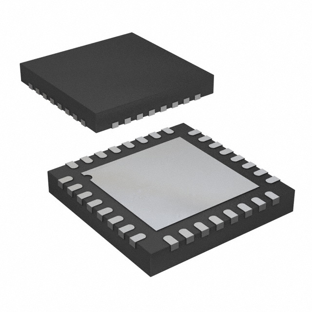
Analog Devices Inc. ADN2815ACPZ
- Part No.:
- ADN2815ACPZ
- Manufacturer:
- Analog Devices Inc.
- Category:
- Application Specific Clock/Timing
- Package:
- 32-WFQFN Exposed Pad, CSP
- Datasheet:
-
 ADN2815ACPZ.pdf
- Description:
- IC CLK DATA REC SDH 1.25GHZ
- Quantity:
- Payment:

- Shipping:

Inventory:3,148
Please send an inquiry. Send us your inquiry, and we will respond immediately.
Product details
Overview
ADN2815ACPZ from Analog Devices is a continuous-rate clock and data recovery (CDR) IC for optical and serial communication receivers, supporting 10 Mb/s to 1.25 Gb/s NRZ data streams without external reference clock, delivering <0.003 UIrms jitter generation at OC-12, LVDS clock/data outputs, and integrated loss-of-lock detection - deployed in SONET OC-12 regenerators and Fibre Channel transceivers.
For engineers reviewing the ADN2815ACPZ datasheet, ADN2815ACPZ pinout, ADN2815ACPZ application, or ADN2815ACPZ equivalent, this page delivers verified technical context, real-world timing behavior, I²C-configurable acquisition modes, jitter tolerance compliance per GR-253-CORE, and validated alternatives for high-reliability telecom signal regeneration designs.
Technical Context
The ADN2815ACPZ implements a hybrid delay-locked loop (DLL) and phase-locked loop (PLL) architecture with shared control voltage: the DLL tracks high-frequency jitter via a voltage-controlled phase shifter (≥2 UI range), while the PLL handles low-frequency components using a VCO with 10 MHz–160 MHz tuning range. Frequency acquisition uses a dedicated frequency detector that resets VCO to 10 MHz and steps coarse tuning until within ±250 ppm of input data rate.
It operates with no reference clock required (autonomous lock), but supports optional REFCLK-assisted locking via I²C-configurable DIV_FREF ratio and frequency band selection (10–20 MHz up to 80–160 MHz); loss-of-lock (LOL) is asserted at ±1000 ppm VCO error and deasserted at ±250 ppm, with static LOL mode available via MISC[4] register bit.
Key Specifications
| Parameter | Value and Actual Design Meaning |
|---|---|
| Data Rate Range | 10 Mb/s to 1.25 Gb/s - supports full SONET OC-1/OC-3/OC-12, GbE, and Fibre Channel without reconfiguration. |
| Jitter Generation | 0.003 UIrms (OC-12, 12 kHz–5 MHz) - meets Telcordia GR-253-CORE for regenerator-grade signal integrity. |
| Jitter Tolerance | 1.0 UIp-p at 250 kHz (OC-12) - exceeds SONET mask requirements for robust operation under stressed input conditions. |
| Output Interface | LVD S differential CLKOUTP/N and DATAOUTP/N - 300 mV typical swing, 100 Ω matched impedance, compatible with standard FPGA/ASIC clock inputs. |
| Power Consumption | 390 mW typical at 1.25 Gb/s - enables dense integration in power-constrained line cards and optical modules. |
| Supply Voltage | 3.3 V ±10% - single-supply operation simplifies board-level power design versus dual-rail CDRs. |
| Operating Temperature | −40°C to +85°C - qualified for industrial and telecom infrastructure environments. |
Pinout & Package
ADN2815ACPZ is housed in a 5 mm × 5 mm, 32-lead LFCSP package with exposed thermal pad (to be soldered to GND). Pin functions are validated per Analog Devices Rev. C datasheet Figure 5 and Table 5.
| Pin/Terminal | Circuit Role | Design Meaning |
|---|---|---|
| VCC (Pins 1,2,12,18,24,31,32) | Power supply input | Seven dedicated VCC pins distribute current across limiting amplifier, VCO, FLL detector, output buffers, and I²C interface - reduces supply noise coupling and improves jitter performance. |
| VEE (Pins 8,13,17,23,30) | Ground return | Five isolated VEE connections separate analog/RF, VCO, FLL, I²C, and phase detector grounds - critical for minimizing ground bounce in high-speed CDR operation. |
| PIN/NIN (Pins 5/4) | Differential CML data input | Internally terminated 50 Ω to 2.5 V VREF; accepts 200 mVp-p min differential swing for BER ≤10−10. |
| CLKOUTP/N (Pins 26/25) | Differential recovered clock output | LVD S-compliant outputs with 300 mV typical swing, 115–220 ps rise/fall time - directly drives SERDES clock inputs without level-shifting. |
| DATAOUTP/N (Pins 29/28) | Differential retimed data output | LVDS outputs aligned to recovered clock edge; supports retiming with sub-400 ps setup/hold (GbE). |
| LOL (Pin 16) | Loss-of-lock indicator | LVTTL active-high open-drain output; asserts at ±1000 ppm VCO error, deasserts at ±250 ppm - provides real-time lock status for system monitoring. |
| SCK/SDA (Pins 20/21) | I²C interface | 400 kHz max clock; enables dynamic configuration of acquisition mode, squelch, output boost, and static LOL - eliminates need for external configuration PROM. |
| CF1/CF2 (Pins 15/14) | Loop filter capacitor terminals | Accepts single 0.47 µF X7R ceramic capacitor - sets VCO tuning bandwidth and determines acquisition time (e.g., 2.0 ms for OC-12). |
Key Features
| Feature | Design Value |
|---|---|
| Autonomous rate detection | Locks to any 10 Mb/s–1.25 Gb/s NRZ stream without reference clock or firmware intervention - reduces BOM and simplifies bring-up in multi-rate systems. |
| Hybrid DLL/PLL architecture | Eliminates jitter peaking (<0.03 dB) by removing zero from closed-loop transfer function - prevents hazardous jitter accumulation in cascaded regenerators. |
| Configurable REFCLK assist | I²C-selectable reference bands (10–20 MHz to 80–160 MHz) and DIV_FREF ratios enable deterministic lock in noisy environments or narrow-data-rate applications. |
| Static LOL monitoring | MISC[4] register bit captures first loss-of-lock event and holds until manually reset - supports fault logging and diagnostics in unattended telecom equipment. |
| Squelch control | LVTTL-active-high SQUELCH (Pin 27) disables both CLKOUT and DATAOUT simultaneously - prevents metastability during link initialization or failure recovery. |
Applications
| SONET OC-12 Regenerator | Fibre Channel Transceiver |
|---|---|
|
Use Scenario: Re-timing degraded OC-12 signals after long-haul fiber transmission with accumulated jitter and amplitude distortion. IC Role / Device Role / Timing Role: Clock and data recovery IC performing quantization, jitter filtering, and retiming of 622.08 Mb/s NRZ data using autonomous DLL/PLL architecture. Use Value: Meets GR-253-CORE jitter generation (<0.003 UIrms) and tolerance (1.0 UIp-p @ 250 kHz), enabling cascade of ≥3 regenerators without exceeding SONET BER limits. |
Use Scenario: Recovering clock and data from 1.0625 Gb/s Fibre Channel links in storage area network switches. IC Role / Device Role / Timing Role: Continuous-rate CDR providing LVDS-aligned clock and retimed data outputs to FC-AL serializer/deserializer. Use Value: 1.25 Gb/s support with 390 mW power enables integration into compact SFP+ modules; I²C programmability allows runtime adaptation to FC-0/FC-1 layer variations. |
| Gigabit Ethernet PHY Interface | WDM Transponder Monitoring |
|
Use Scenario: Extracting clean clock and data from 1.25 Gb/s GbE serial streams in switch fabric line cards. IC Role / Device Role / Timing Role: Standalone CDR generating low-jitter LVDS clock (CLKOUTP/N) and retimed data (DATAOUTP/N) synchronized to IEEE 802.3 jitter tolerance mask. Use Value: 637 kHz jitter tolerance (0.749 UIp-p) ensures reliable operation under worst-case GbE jitter stress; 400 ps setup/hold margin simplifies FPGA interface timing closure. |
Use Scenario: Real-time monitoring of multiple WDM channel data rates and lock status in optical transport platforms. IC Role / Device Role / Timing Role: CDR with I²C-accessible coarse data rate readback (±10%) and LOL status reporting for remote diagnostics. Use Value: Coarse readback register (0x3) and static LOL bit (MISC[4]) enable software-based channel health assessment without external test equipment. |
Equivalent & Alternatives
The following parts are listed as comparable options for similar clock and data recovery applications.
| Alternative Part | Technical Difference | Application Difference | Selection Advice |
|---|---|---|---|
| MAX3675ETJ+ | Fixed-rate CDR (1.25 Gb/s only); no autonomous rate detection; requires external reference clock for lock; 3.3 V supply; 32-pin TQFN. | Only suitable for single-rate GbE or Fibre Channel systems; cannot replace ADN2815ACPZ in multi-rate SONET OC-1/OC-3/OC-12 deployments. | Select when cost-sensitive, fixed-rate applications eliminate need for wide-range autonomy and I²C configurability. |
| LMK03806RHAT | Programmable clock generator with integrated CDR (10 Mb/s–3.2 Gb/s); includes on-chip VCO, jitter cleaner, and SPI interface; 40-pin QFN. | Higher integration (clock synthesis + CDR) but larger footprint and higher power (650 mW); lacks LOL pin and autonomous lock simplicity. | Select when system requires programmable clock outputs alongside CDR, and board space/power budget permits added complexity. |
Compared with MAX3675ETJ+, ADN2815ACPZ enables seamless multi-rate interoperability without hardware changes; compared with LMK03806RHAT, it offers lower power, smaller footprint, and simpler lock management - making it optimal for space-constrained, autonomous telecom receiver stages.
Availability
ADN2815ACPZ is available at Aetrix Electronics and suitable for SONET regenerators, Fibre Channel transceivers, and Gigabit Ethernet PHY interfaces requiring stable component supply, long-term lifecycle assurance, and traceable sourcing for telecom infrastructure programs.
Supply support for ADN2815ACPZ includes scheduled delivery planning, volume procurement assistance, BOM continuity management, traceable sourcing, and lifecycle availability coordination for OEM customers, industrial embedded developers, connected-device designers, and electronics production programs.
Manufacturer
Analog Devices is a global leader in high-performance analog, mixed-signal, and digital signal processing semiconductors, serving precision instrumentation, industrial automation, and communications markets since 1965.
The ADN2815ACPZ belongs to Analog Devices' Clock and Timing product line, engineered specifically for carrier-grade optical receiver subsystems requiring ultra-low jitter, autonomous multi-rate operation, and robust lock monitoring in harsh thermal environments.
FAQ
What data rates does the ADN2815ACPZ support without external configuration?
The ADN2815ACPZ supports continuous-rate operation from 10 Mb/s to 1.25 Gb/s with no external reference clock or programming required. It autonomously acquires and locks to any NRZ data stream in this range using its internal frequency detector and hybrid DLL/PLL architecture - confirmed by datasheet Table 1 and General Description section. This makes ADN2815ACPZ ideal for multi-standard systems like SONET OC-1/OC-3/OC-12 where rate changes occur dynamically.
Does the ADN2815ACPZ require an external loop filter capacitor?
Yes, the ADN2815ACPZ requires a single 0.47 µF ±20% X7R ceramic capacitor connected between CF1 (Pin 15) and CF2 (Pin 14) to set the VCO tuning bandwidth and stabilize frequency acquisition. The datasheet specifies leakage current <10 nA and insulation resistance >300 MΩ to prevent drift in acquisition time - omission or substitution invalidates jitter performance and lock reliability for ADN2815ACPZ.
How does the loss-of-lock (LOL) indicator behave on the ADN2815ACPZ?
The LOL pin (Pin 16) on ADN2815ACPZ is an LVTTL active-high output that asserts when VCO frequency error exceeds ±1000 ppm and deasserts when error falls within ±250 ppm - providing hysteresis to prevent chatter. It can also be configured as a static indicator (via CTRLB[7]) that remains asserted after first loss-of-lock until manually reset through I²C register CTRLB[6], enabling persistent fault logging in ADN2815ACPZ-based systems.
Can the ADN2815ACPZ be used with a reference clock for faster lock acquisition?
Yes, the ADN2815ACPZ supports optional REFCLK-assisted locking via differential REFCLKP/REFCLKN inputs (Pins 10/11). When enabled via I²C register CTRLA[0], it uses user-configured frequency bands (10–20 MHz to 80–160 MHz) and DIV_FREF ratios to accelerate acquisition - reducing lock time to 20.0 ms versus up to 40.0 ms in autonomous mode. This mode is validated in the Functional Description section and Table 8 of the ADN2815ACPZ datasheet.
What output standards are supported by the ADN2815ACPZ clock and data outputs?
The ADN2815ACPZ provides LVDS-compliant differential outputs on CLKOUTP/N (Pins 26/25) and DATAOUTP/N (Pins 29/28), with 300 mV typical differential swing, 100 Ω output impedance, and 115–220 ps rise/fall times. These outputs meet ANSI/TIA/EIA-644-A LVDS specifications and are designed to drive standard FPGA, ASIC, or SERDES clock/data inputs directly - no level-shifting or termination redesign needed for ADN2815ACPZ integration.
ADN2815ACPZ Specifications
- Product attributes
- Attribute value
- Manufacturer:
- Analog Devices Inc.
- Series:
- -
- Package/Case:
- 32-WFQFN Exposed Pad, CSP
- Packaging:
- Bulk
- Product Status:
- Active
- Programmable:
- Not Verified
- PLL:
- Yes
- Main Purpose:
- SONET/SDH
- Input:
- CML
- Output:
- LVDS
- Number of Circuits:
- 1
- Ratio - Input:Output:
- 1:2
- Differential - Input:Output:
- Yes/Yes
- Frequency - Max:
- 1.25GHz
- Voltage - Supply:
- 3V ~ 3.6V
- Operating Temperature:
- -40°C ~ 85°C
- Mounting Type:
- Surface Mount
- Grade:
- -
- Qualification:
- -
- Supplier Device Package:
- 32-LFCSP-WQ (5x5)
ADN2815ACPZ FAQ
1.How can I place an order for ADN2815ACPZ through Aetrix?
Please submit a Request for Quotation (RFQ) for ADN2815ACPZ on Aetrix. Our sales agent will provide a competitive quotation and guide you through the order confirmation once you accept the terms.
2.Are the price and stock information for ADN2815ACPZ reliable?
The price and inventory of ADN2815ACPZ are updated periodically and may fluctuate due to market conditions. Stock and pricing data are typically refreshed every 24 hours. Quotation validity for ADN2815ACPZ is usually 5 days.
3.What payment methods are accepted for ADN2815ACPZ?
We accept Wire Transfer, PayPal, Credit Card, Western Union, MoneyGram, and Escrow for ADN2815ACPZ transactions.
Note: Certain payment methods may incur a processing fee.
4.How is shipping managed for ADN2815ACPZ?
ADN2815ACPZ orders can be shipped via leading logistics carriers, including DHL, UPS, FedEx, TNT, or Registered Mail.
Once your ADN2815ACPZ order is processed, you will receive an email with the shipment details and tracking number.
Note: Tracking information may take up to 24 hours to appear. Express delivery typically takes 3–5 business days.
5.How can I obtain technical support or documentation for ADN2815ACPZ?
For technical support, including ADN2815ACPZ datasheets, pinout diagrams, or application guidance, please contact our engineering support team. They can provide detailed documentation and assistance for your ADN2815ACPZ requirements.
6.How does Aetrix verify that ADN2815ACPZ is sourced from the original manufacturer or authorized distributors?
All ADN2815ACPZ products on Aetrix are procured from qualified distributors and authorized channels. Our dedicated quality assurance team conducts strict verification, including traceability checks and, if necessary, third-party testing. This ensures that ADN2815ACPZ meets industry standards.
7.What is the process for return or replacement of ADN2815ACPZ?
All ADN2815ACPZ units undergo pre-shipment inspection (PSI). If there is an issue with ADN2815ACPZ, returns or replacements are accepted under the following conditions:
1.Quantity discrepancies, incorrect items, or visible external defects (such as breakage or corrosion), acknowledged by Aetrix.
2.The issue is reported within 90 days of delivery.
3.The ADN2815ACPZ part is unused and in its original packaging.
Return procedure for ADN2815ACPZ:
1.Submit a request within 90 days.
2.Obtain a Return Material Authorization (RMA) from Aetrix.
ADN2815ACPZ Tags
-
LMK00334RTVRQ1
Texas Instruments
.jpg)
-
DSC557-0344FI0T
Microchip Technology
-
9FGV0241AKILFT
Renesas

-
9DBL0452CKILFT
Renesas
-
DSC557-0344FL1T
Microchip Technology
-
RC19008AGND#KB0
Renesas
-
RC19008AGND#BB0
Renesas

-
9DB403DGILFT
Renesas
-
9DB233AGILFT
Renesas

-
9DB803DGILFT
Renesas
-
9FGL0851DKILFT
Renesas
-
AB-557-03-HCHC-F-L-C-T
Abracon LLC
Tech Hub

A practical engineering guide to 3.3V and 5V logic compatibility, input thresholds, resistor dividers, translator ICs, MOSFET level shifting, I2C pull-ups, timing limits and power-sequencing risks.

The 74HC595 uses push-pull logic outputs, while the TPIC6B595 uses 50 V open-drain DMOS sinks for higher-power loads. This guide compares timing, current limits, 3.3 V interfacing, load wiring, thermal…

The 74HC595 converts serial data into eight stable parallel outputs. This guide covers pin functions, shift and storage timing, OE and MR behavior, drive-current limits, cascading, voltage compatibilit…

A technical comparison of level-sensitive latches and edge-triggered flip-flops, covering timing windows, setup and hold limits, master–slave operation, time borrowing, race-through, HDL inference and…

A D latch stores one bit while Enable controls when data can pass. This reference covers gate-level operation, truth tables, transparency, setup and hold timing, LE versus OE, common ICs and practical …

An SR latch stores one bit through cross-coupled feedback. This engineering reference covers NOR and NAND implementations, truth tables, forbidden-state recovery, gated operation, switch debouncing, fa…

Latch circuits retain one bit through feedback. This technical reference covers SR and D latches, truth tables, transparency, timing limits, latch-versus-flip-flop behavior, applications and common log…

An engineering guide to LED driver operation, constant-current and constant-voltage outputs, linear and switching topologies, dimming, IC selection, calculations, replacement compatibility, and fault c…

Operational amplifier guide covering op amp basics, feedback, ideal vs real op amps, common configurations, buffer circuits, offset, bias current, gain-bandwidth, slew rate, rail-to-rail limits and sel…

Jumper cables guide covering safe connection order, red and black clamp placement, final ground connection, cable gauge, length, clamp quality, copper vs CCA cables, jump starter comparison and battery…


