
 My Inquiry
 My Account


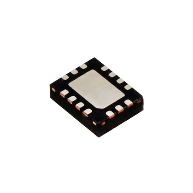
Analog Devices Inc. ADN2819ACPZ-CML-RL
.jpg)
- Part No.:
- ADN2819ACPZ-CML-RL
- Manufacturer:
- Analog Devices Inc.
- Category:
- Application Specific Clock/Timing
- Package:
- 48-WFQFN Exposed Pad, CSP
- Datasheet:
-
 ADN2819ACPZ-CML-RL.pdf
- Description:
- IC CLOCK/DATA RECOVERY 48LFCSP
- Quantity:
- Payment:

- Shipping:

Inventory:4,037
Please send an inquiry. Send us your inquiry, and we will respond immediately.
Product details
Overview
ADN2819ACPZ-CML-RL from Analog Devices is a multirate clock and data recovery (CDR) IC with integrated limiting amplifier, supporting 2.7 Gbps operation for SONET OC-48/SDH STM-16, Gigabit Ethernet, and 15/14 FEC rates. It delivers jitter transfer ≤880 kHz, jitter generation as low as 0.002 UI rms, and loss-of-signal detection down to 3 mV. Used in fiber-optic receiver front ends with PIN diode and TIA.
For engineers reviewing the ADN2819ACPZ-CML-RL datasheet, ADN2819ACPZ-CML-RL pinout, ADN2819ACPZ-CML-RL application, or ADN2819ACPZ-CML-RL equivalent, key selection criteria include CML output compatibility, 7 mm × 7 mm 48-lead LFCSP package, reference clock flexibility (19.44–155.52 MHz), adjustable slice level (±100 mV), and guaranteed SONET-compliant jitter performance across OC-3/OC-12/OC-48 rates.
Technical Context
The ADN2819ACPZ-CML-RL implements a hybrid delay-locked loop (DLL) and phase-locked loop (PLL) architecture to simultaneously achieve wideband jitter accommodation and narrow-band jitter filtering. Its dual-loop design separates high-frequency jitter tracking (via voltage-controlled phase shifter) from low-frequency tracking (via VCO), eliminating closed-loop zeros and minimizing jitter peaking.
It supports native and 15/14 digital wrapper rates using a single reference clock frequency - selectable among 19.44 MHz, 38.88 MHz, 77.76 MHz, or 155.52 MHz - with LVPECL/LVDS/LVCMOS/LVTTL-compatible REFCLK inputs. The on-chip oscillator enables crystal-based timing when external REFCLK is unavailable.
Key Specifications
| Parameter | Value and Actual Design Meaning |
|---|---|
| Max Data Rate | 2.7 Gbps - supports OC-48 (2.488 Gbps), GbE (1.25 Gbps), and 15/14 FEC rates without reconfiguration. |
| Jitter Generation | 0.002 UI rms (OC-3/OC-12) - ensures minimal added timing uncertainty in regenerated data streams. |
| Input Sensitivity | 4 mV p-p typical - enables reliable recovery from low-amplitude optical signals after TIA amplification. |
| Bandwidth | 1.9 GHz - preserves signal integrity for NRZ data up to 2.7 Gbps with <10 ps pulse width distortion. |
| Supply Voltage | 3.3 V ±10% - single-supply operation simplifies power delivery in dense line-card designs. |
| Power Dissipation | 540 mW typical - low thermal load supports compact 7 mm × 7 mm LFCSP packaging in thermally constrained modules. |
| LOS Threshold Range | 0.7–18.0 mV - programmable via THRADJ resistor to match varying front-end gain and noise floor. |
Pinout & Package
The ADN2819ACPZ-CML-RL is housed in a 7 mm × 7 mm, 48-lead lead-frame chip-scale package (LFCSP) with exposed paddle soldered to VCC. Pin 1 is marked by a dot; the exposed pad (EPAD) must be connected to VCC via multiple vias for thermal and electrical performance.
| Pin/Terminal | Circuit Role | Design Meaning |
|---|---|---|
| PIN / NIN | Differential Data Input | AC-coupled NRZ input pair accepting 4 mV p-p minimum; common-mode ~0.6 V for optimal sensitivity. |
| CLKOUTP/N | Differential Recovered Clock Output | CML-compatible outputs with 600–1200 mV differential swing; 150 ps rise/fall time for clean clock distribution. |
| DATAOUTP/N | Differential Retimed Data Output | CML outputs synchronized to recovered clock; setup/hold times as low as 140 ps (OC-48) enable direct interface to downstream logic. |
| REFCLKP/N | Differential Reference Clock Input | Accepts 19.44–155.52 MHz LVPECL/LVDS/LVCMOS/LVTTL; LVPECL/LVDS only at 155.52 MHz per datasheet. |
| THRADJ | LOS Threshold Programming | Connects external resistor to set SDOUT trip point between 0.7 mV and 18.0 mV - critical for stable signal detect in low-SNR links. |
| LOL | Loss of Lock Indicator | LVTTL active-high output signaling PLL unlock condition; used for system fault monitoring and automatic switchover. |
Key Features
| Feature | Design Value |
|---|---|
| Patented DLL+PLL Architecture | Eliminates jitter peaking by removing closed-loop zero - achieves <0.025 dB peaking vs. >3 dB in conventional PLLs. |
| Adjustable Slice Level | ±100 mV fine-tuning range allows optimization for varying input amplitude and baseline wander in long-haul links. |
| Integrated LOS Detector | Hysteresis-programmable (3.2–9.9 dB) prevents chatter during marginal signal conditions; response time <0.3 μs (dc-coupled). |
| Multirate Reference Flexibility | Single REFCLK frequency supports OC-3/OC-12/OC-48/GbE/15/14 FEC - eliminates need for multiple clock sources or rate-switching logic. |
| On-Chip Oscillator | 19.44 MHz crystal oscillator enables self-contained timing when external REFCLK is unavailable - reduces BOM count and board space. |
Applications
| SONET/SDH Regenerator | WDM Transponder Receiver |
|---|---|
Use Scenario: Re-timing degraded OC-48 signals in metro/regional optical networks where accumulated jitter exceeds ITU-T G.823 limits. IC Role / Device Role / Timing Role: Clock and data recovery IC providing jitter cleanup, signal retiming, and loss-of-signal monitoring in the receive path. Use Value: Meets Telcordia GR-253 SONET jitter transfer/generation/tolerance specs - enables cascade of ≥5 regenerators without hazardous jitter accumulation. | Use Scenario: Front-end CDR in dual-channel 10G WDM transponders requiring independent timing recovery for each wavelength. IC Role / Device Role / Timing Role: Multirate CDR with integrated limiting amplifier, enabling direct connection to TIAs without external gain stages. Use Value: 4 mV p-p sensitivity and 1.9 GHz bandwidth support low-power, high-density receiver modules with <540 mW total dissipation. |
| Gigabit Ethernet Backplane | Optical Test Equipment |
Use Scenario: Recovering and retiming 1.25 Gbps data from FR4 backplanes with >20 dB channel loss and intersymbol interference. IC Role / Device Role / Timing Role: CDR with bypass and loopback modes for production test and field diagnostics. Use Value: Loopback mode enables high-speed bit-error-rate testing without external pattern generators; squelch/bypass features simplify system-level validation. | Use Scenario: Embedded CDR in modular optical test sets performing jitter tolerance, transfer, and generation measurements per GR-253. IC Role / Device Role / Timing Role: Reference-grade CDR with calibrated jitter performance and programmable reference clock selection. Use Value: Jitter generation <0.003 UI rms (OC-48) and tolerance mask compliance up to 92 UI p-p (600 Hz) provide traceable metrology-grade timing recovery. |
Equivalent & Alternatives
The following parts are listed as comparable options for similar clock and data recovery applications.
| Alternative Part | Technical Difference | Application Difference | Selection Advice |
|---|---|---|---|
| MAX3795ETJ+ | Supports up to 3.2 Gbps; requires separate limiting amplifier; no on-chip oscillator; uses 5 mm × 5 mm TQFN. | Better suited for higher-rate 10G Ethernet but lacks integrated limiter and crystal oscillator - increases component count. | Select MAX3795ETJ+ only if >2.7 Gbps operation is required and external limiter/oscillator integration is acceptable. |
| LMH0384SQ/NOPB | Designed for SMPTE serial digital video (2.97 Gbps); different jitter mask (SMPTE ST 292); no 15/14 FEC support; LVDS outputs only. | Targeted at broadcast video infrastructure - not compliant with SONET/SDH jitter specs or telecom FEC rates. | LMH0384SQ/NOPB is unsuitable for telecom applications; use only in video timing systems requiring SMPTE compliance. |
Compared with MAX3795ETJ+ and LMH0384SQ/NOPB, the ADN2819ACPZ-CML-RL uniquely integrates limiting amplification, on-chip oscillator, and SONET-compliant jitter performance in a single 7 mm × 7 mm package - reducing bill-of-materials and layout complexity for OC-3/OC-12/OC-48 systems.
Availability
ADN2819ACPZ-CML-RL is available at Aetrix Electronics and suitable for SONET regenerators, WDM transponder receivers, Gigabit Ethernet backplanes, and optical test equipment requiring stable component supply, long-term lifecycle support, and guaranteed SONET jitter compliance.
Supply support for ADN2819ACPZ-CML-RL includes scheduled delivery planning, volume procurement assistance, BOM continuity management, traceable sourcing, and lifecycle availability coordination for OEM customers, industrial embedded developers, connected-device designers, and electronics production programs.
Manufacturer
Analog Devices, Inc. is a global semiconductor company specializing in high-performance analog, mixed-signal, and digital signal processing technologies for precision instrumentation, communications, and industrial applications.
The ADN2819ACPZ-CML-RL belongs to Analog Devices' clock and data recovery product line, engineered specifically for telecom and datacom applications demanding SONET/SDH-compliant jitter performance, multirate flexibility, and integration of limiting amplification in compact packages.
FAQ
What reference clock frequencies does the ADN2819ACPZ-CML-RL support?
The ADN2819ACPZ-CML-RL supports four fixed reference clock frequencies: 19.44 MHz, 38.88 MHz, 77.76 MHz, and 155.52 MHz. These correspond to SONET OC-1/OC-3/OC-12/OC-48 base rates and their harmonics. The device uses a single REFCLK for all supported data rates including 15/14 FEC wrappers - no clock switching or reconfiguration is needed when changing data rates. LVPECL and LVDS inputs are only valid at 155.52 MHz per the datasheet.
Does the ADN2819ACPZ-CML-RL require an external limiting amplifier?
No, the ADN2819ACPZ-CML-RL includes an integrated limiting amplifier as part of its signal chain. This eliminates the need for an external limiter stage when interfacing with transimpedance amplifiers (TIAs) in optical receiver modules. The quantizer input sensitivity of 4 mV p-p (typical) is specified with the internal limiter enabled, and the device is designed to operate directly after a TIA in standard fiber-optic receiver architectures.
How is loss-of-signal (LOS) detection configured on the ADN2819ACPZ-CML-RL?
LOS detection on the ADN2819ACPZ-CML-RL is configured via the THRADJ pin, which accepts an external resistor to set the SDOUT trip threshold between 0.7 mV and 18.0 mV depending on resistance value (2 Ω to 90 kΩ). Hysteresis is programmable from 3.2 dB to 9.9 dB based on RTHRESH and data rate. The SDOUT output is an active-high LVTTL signal with <0.3 μs response time under dc-coupled conditions, and includes built-in hysteresis to prevent chatter near threshold.
What are the key jitter specifications met by the ADN2819ACPZ-CML-RL?
The ADN2819ACPZ-CML-RL meets Telcordia GR-253-CORE SONET/SDH requirements for jitter transfer, generation, and tolerance across OC-3, OC-12, OC-48, and GbE rates. Key values include jitter transfer bandwidths of 48–880 kHz, jitter generation as low as 0.002 UI rms, and jitter tolerance up to 92 UI p-p at 600 Hz (OC-48). All jitter specs are guaranteed over –40°C to +85°C ambient temperature.
Can the ADN2819ACPZ-CML-RL operate without an external reference clock?
Yes, the ADN2819ACPZ-CML-RL can operate without an external reference clock by enabling its on-chip 19.44 MHz oscillator using an external crystal connected to XO1/XO2 pins. The REFSEL pin selects between internal oscillator (REFSEL = 0) and external REFCLK (REFSEL = 1). When using the internal oscillator, the device still supports all multirate functions - including OC-48 and 15/14 FEC - without requiring external clock synthesis.
ADN2819ACPZ-CML-RL Specifications
- Product attributes
- Attribute value
- Manufacturer:
- Analog Devices Inc.
- Series:
- -
- Package/Case:
- 48-WFQFN Exposed Pad, CSP
- Packaging:
- Tape & Reel (TR)
- Product Status:
- Obsolete
- Programmable:
- Not Verified
- PLL:
- Yes
- Main Purpose:
- SONET/SDH, STM
- Input:
- CML
- Output:
- CML
- Number of Circuits:
- 1
- Ratio - Input:Output:
- 1:2
- Differential - Input:Output:
- Yes/Yes
- Frequency - Max:
- 2.7GHz
- Voltage - Supply:
- 3V ~ 3.6V
- Operating Temperature:
- -40°C ~ 85°C
- Mounting Type:
- Surface Mount
- Grade:
- -
- Qualification:
- -
- Supplier Device Package:
- 48-LFCSP (7x7)
ADN2819ACPZ-CML-RL FAQ
1.How can I place an order for ADN2819ACPZ-CML-RL through Aetrix?
Please submit a Request for Quotation (RFQ) for ADN2819ACPZ-CML-RL on Aetrix. Our sales agent will provide a competitive quotation and guide you through the order confirmation once you accept the terms.
2.Are the price and stock information for ADN2819ACPZ-CML-RL reliable?
The price and inventory of ADN2819ACPZ-CML-RL are updated periodically and may fluctuate due to market conditions. Stock and pricing data are typically refreshed every 24 hours. Quotation validity for ADN2819ACPZ-CML-RL is usually 5 days.
3.What payment methods are accepted for ADN2819ACPZ-CML-RL?
We accept Wire Transfer, PayPal, Credit Card, Western Union, MoneyGram, and Escrow for ADN2819ACPZ-CML-RL transactions.
Note: Certain payment methods may incur a processing fee.
4.How is shipping managed for ADN2819ACPZ-CML-RL?
ADN2819ACPZ-CML-RL orders can be shipped via leading logistics carriers, including DHL, UPS, FedEx, TNT, or Registered Mail.
Once your ADN2819ACPZ-CML-RL order is processed, you will receive an email with the shipment details and tracking number.
Note: Tracking information may take up to 24 hours to appear. Express delivery typically takes 3–5 business days.
5.How can I obtain technical support or documentation for ADN2819ACPZ-CML-RL?
For technical support, including ADN2819ACPZ-CML-RL datasheets, pinout diagrams, or application guidance, please contact our engineering support team. They can provide detailed documentation and assistance for your ADN2819ACPZ-CML-RL requirements.
6.How does Aetrix verify that ADN2819ACPZ-CML-RL is sourced from the original manufacturer or authorized distributors?
All ADN2819ACPZ-CML-RL products on Aetrix are procured from qualified distributors and authorized channels. Our dedicated quality assurance team conducts strict verification, including traceability checks and, if necessary, third-party testing. This ensures that ADN2819ACPZ-CML-RL meets industry standards.
7.What is the process for return or replacement of ADN2819ACPZ-CML-RL?
All ADN2819ACPZ-CML-RL units undergo pre-shipment inspection (PSI). If there is an issue with ADN2819ACPZ-CML-RL, returns or replacements are accepted under the following conditions:
1.Quantity discrepancies, incorrect items, or visible external defects (such as breakage or corrosion), acknowledged by Aetrix.
2.The issue is reported within 90 days of delivery.
3.The ADN2819ACPZ-CML-RL part is unused and in its original packaging.
Return procedure for ADN2819ACPZ-CML-RL:
1.Submit a request within 90 days.
2.Obtain a Return Material Authorization (RMA) from Aetrix.
ADN2819ACPZ-CML-RL Tags
-
LMK00334RTVRQ1
Texas Instruments
.jpg)
-
DSC557-0344FI0T
Microchip Technology
-
9FGV0241AKILFT
Renesas

-
9DBL0452CKILFT
Renesas
-
DSC557-0344FL1T
Microchip Technology
-
RC19008AGND#KB0
Renesas
-
RC19008AGND#BB0
Renesas

-
9DB403DGILFT
Renesas
-
9DB233AGILFT
Renesas

-
9DB803DGILFT
Renesas
-
9FGL0851DKILFT
Renesas
-
AB-557-03-HCHC-F-L-C-T
Abracon LLC
Tech Hub

A practical engineering guide to 3.3V and 5V logic compatibility, input thresholds, resistor dividers, translator ICs, MOSFET level shifting, I2C pull-ups, timing limits and power-sequencing risks.

The 74HC595 uses push-pull logic outputs, while the TPIC6B595 uses 50 V open-drain DMOS sinks for higher-power loads. This guide compares timing, current limits, 3.3 V interfacing, load wiring, thermal…

The 74HC595 converts serial data into eight stable parallel outputs. This guide covers pin functions, shift and storage timing, OE and MR behavior, drive-current limits, cascading, voltage compatibilit…

A technical comparison of level-sensitive latches and edge-triggered flip-flops, covering timing windows, setup and hold limits, master–slave operation, time borrowing, race-through, HDL inference and…

A D latch stores one bit while Enable controls when data can pass. This reference covers gate-level operation, truth tables, transparency, setup and hold timing, LE versus OE, common ICs and practical …

An SR latch stores one bit through cross-coupled feedback. This engineering reference covers NOR and NAND implementations, truth tables, forbidden-state recovery, gated operation, switch debouncing, fa…

Latch circuits retain one bit through feedback. This technical reference covers SR and D latches, truth tables, transparency, timing limits, latch-versus-flip-flop behavior, applications and common log…

An engineering guide to LED driver operation, constant-current and constant-voltage outputs, linear and switching topologies, dimming, IC selection, calculations, replacement compatibility, and fault c…

Operational amplifier guide covering op amp basics, feedback, ideal vs real op amps, common configurations, buffer circuits, offset, bias current, gain-bandwidth, slew rate, rail-to-rail limits and sel…

Jumper cables guide covering safe connection order, red and black clamp placement, final ground connection, cable gauge, length, clamp quality, copper vs CCA cables, jump starter comparison and battery…


