
 My Inquiry
 My Account


Analog Devices Inc. ADN2847ACPZ-32
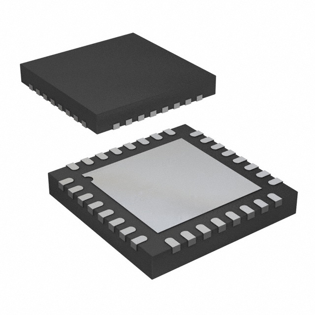
- Part No.:
- ADN2847ACPZ-32
- Manufacturer:
- Analog Devices Inc.
- Category:
- Laser Drivers
- Package:
- 32-WFQFN Exposed Pad, CSP
- Datasheet:
-
 ADN2847ACPZ-32.pdf
- Description:
- IC LASER DRVR 3.3GB 3.6V 32LFCSP
- Quantity:
- Payment:

- Shipping:

Inventory:3,032
Please send an inquiry. Send us your inquiry, and we will respond immediately.
Product details
Overview
ADN2847ACPZ-32 from Analog Devices is a 3.3 V dual-loop laser diode driver IC supporting 50 Mbps to 3.3 Gbps data rates, delivering bias current up to 100 mA and modulation current up to 80 mA with 80 ps typical rise/fall time. It integrates closed-loop average optical power and extinction ratio control for SONET/SDH compliance in fiber-optic transmitters.
For engineers reviewing the ADN2847ACPZ-32 datasheet, ADN2847ACPZ-32 pinout, ADN2847ACPZ-32 application, or ADN2847ACPZ-32 equivalent, key selection criteria include its 32-lead LFCSP package, dual MPD monitoring capability (limited to 48-lead variant), ALS alarm interface, and support for DWDM wavelength control via ERSET/PSET analog tuning.
Technical Context
The ADN2847ACPZ-32 implements two independent closed-loop control paths: one for average optical power (via PSET and IMPD feedback) and another for extinction ratio (via ERSET and dual-MPD current summation). Its control architecture uses analog voltage-set resistive networks and internal current mirrors (IBMON, IMMON, IMPDMON) to enable real-time bias/modulation adjustment without external DACs or microcontrollers.
It supports both ac-coupled and dc-coupled laser interfacing, with configurable loop bandwidth via LBWSET and external PAVCAP/ERCAP capacitors. The device includes programmable laser fail/degrade alarms referenced to ASET, automatic laser shutdown (ALS), and optional clocked data input via CLKSEL, DATAP/DATAN, and CLKP/CLKN differential pairs.
Key Specifications
| Parameter | Value and Actual Design Meaning |
|---|---|
| Data Rate Range | 50 Mbps to 3.3 Gbps - supports OC-48/STM-16 and Gigabit Ethernet physical layer timing |
| Bias Current Range | 2 mA to 100 mA - sufficient for edge-emitting lasers in SFP/SFF modules |
| Modulation Current Range | 5 mA to 80 mA - enables high extinction ratio (>10 dB) at 3.3 Gbps |
| Rise/Fall Time | 80 ps typical - preserves signal integrity for NRZ eye opening at 2.5+ Gbps |
| Supply Voltage | 3.0 V to 3.6 V - single-rail operation compatible with standard 3.3 V telecom power domains |
| Monitor PD Current | 50 μA to 1200 μA - accommodates wide dynamic range of monitor photodiodes |
| Alarm Threshold Setting | 1.2 kΩ to 25 kΩ on ASET - sets FAIL/DEGRADE thresholds with 10% hysteresis |
Pinout & Package
ADN2847ACPZ-32 is housed in a 32-lead, 5 mm × 5 mm LFCSP package with exposed thermal pad (EPAD) requiring connection to VCC or ground plane per datasheet Figure 8. Pin count and function mapping differ from the 48-lead variant; dual MPD (IMPD2/IMPDMON2) and IDTONE are omitted.
| Pin/Terminal | Circuit Role | Design Meaning |
|---|---|---|
| LBWSET (Pin 1) | Loop Bandwidth Select | Logic-high selects 1 μF PAVCAP/ERCAP for continuous 50 Mbps–3.3 Gbps operation |
| ASET (Pin 2) | Alarm Threshold Reference | Sets FAIL/DEGRADE trip points via external resistor; 100:1 current ratio to IFAIL |
| ERSET (Pin 3) | Extinction Ratio Set | Analog input (1.1–1.3 V) defining target ER = P1/P0 via RERSET potentiometer |
| PSET (Pin 4) | Average Power Set | Analog input (1.1–1.3 V) defining target PAV = (P1 + P0)/2 via RPSET potentiometer |
| IMPD (Pin 5) | Monitor Photodiode Input | Primary feedback node for APC loop; accepts 50–1200 μA photodiode current |
| IMPDMON (Pin 6) | MPD Current Mirror Output | 1:1 mirrored current for external monitoring or calibration; compliance up to VCC − 1.2 V |
| GND4 (Pin 7) | Supply Ground | Dedicated ground return for analog sensing circuitry; separate from power grounds |
| VCC4 (Pin 8) | Supply Voltage | One of four VCC pins; must be shorted to other VCC pins and bypassed locally |
| ERCAP (Pin 9) | Extinction Ratio Loop Capacitor | Connects to ground to set ER loop time constant; value selected per LBWSET mode |
| PAVCAP (Pin 10) | Average Power Loop Capacitor | Connects to ground to set APC loop time constant; value matched to ERCAP |
| VCC1 (Pin 11) | Supply Voltage | Second dedicated VCC pin; requires local 100 nF + 10 nF decoupling |
| DATAN (Pin 12) | Data Negative Input | Differential data input (ac-coupled); 50 Ω termination internal to chip |
| DATAP (Pin 13) | Data Positive Input | Differential data input (ac-coupled); common-mode voltage self-biased |
| GND1 (Pin 14) | Supply Ground | Ground return for data/clock inputs; isolated from analog sensing grounds |
| CLKP (Pin 15) | Clock Positive Input | Optional differential clock input used only when CLKSEL = VCC |
| CLKN (Pin 16) | Clock Negative Input | Paired with CLKP; unused if CLKSEL = GND (data-only mode) |
| CCBIAS (Pin 32) | Extra Bias Control | Connected to VCC for dc-coupled lasers; tied to IBIAS for ac-coupled configuration |
| IBIAS (Pins 31, 47) | Laser Bias Current Output | High-current output driving LD cathode; compliance voltage ≥1.2 V |
| IMODP (Pins 28, 42) | Modulation Current Positive | Drives LD anode; connects directly to laser diode in dc-coupled topology |
| IMODN (Pins 26, 39) | Modulation Current Negative | Returns modulation current via matching resistor to VCC; defines differential swing |
| ALS (Pin 20) | Automatic Laser Shutdown | Active-high input forcing IBIAS/IMOD to <0.1 mA; triggers FAIL alarm |
| FAIL (Pin 19) | Laser Fail Alarm Output | Open-drain active-high output with 30 kΩ internal pull-up to VCC |
| DEGRADE (Pin 18) | Laser Degrade Alarm Output | Open-drain active-high output asserted at 90% of FAIL threshold |
| CLKSEL (Pin 17) | Clock Select | Logic-high enables clocked data mode; logic-low enables data-only (clock recovery not supported) |
| IBMON (Pin 24) | Bias Current Mirror Output | 100× scaled replica of IBIAS for external monitoring; compliance up to VCC − 1.2 V |
| IMMON (Pin 23) | Modulation Current Mirror Output | 100× scaled replica of IMOD for external monitoring; matches IBMON division ratio |
| VCC2 (Pin 25) | Supply Voltage | Third VCC pin; shares same rail as VCC1/VCC3/VCC4 |
| VCC3 (Pin 21) | Supply Voltage | Fourth VCC pin; all VCC pins must be shorted and individually bypassed |
| GND2 (Pins 27, 29, 30, 34, 35, 36, 40, 41, 44, 45) | Supply Ground | Multiple dedicated ground pins distributed across package for low-inductance return paths |
| GND3 (Pin 22) | Supply Ground | Ground return for alarm outputs and CLKSEL; electrically distinct from GND1/GND4 |
Key Features
| Feature | Design Value |
|---|---|
| Dual closed-loop control | Simultaneous APC and ERC loops eliminate need for external compensation circuits or temperature sensors |
| Programmable laser alarms | FAIL and DEGRADE outputs meet ITU-T G.958 transmitter failure/degradation requirements |
| Full current parameter monitoring | IBMON, IMMON, IMPDMON provide scalable analog voltage outputs for system-level diagnostics |
| Low-component-count interface | Only external components required are PSET/ERSET/ASET resistors, PAVCAP/ERCAP capacitors, and RZ pull-up |
| Robust laser protection | ALS input forces immediate current shutdown; internal compliance limits prevent overvoltage damage to LD |
Applications
| SONET/SDH Transmitter | Fibre Channel Link |
|---|---|
Use Scenario: OC-48/STM-16 line card in metro optical network requiring stable 2.488 Gbps transmission over temperature. IC Role / Device Role / Timing Role: Laser diode driver providing closed-loop power and extinction ratio control to maintain BER <1e−12. Use Value: Eliminates manual calibration and aging drift; meets GR-468 reliability standards without external DACs. |
Use Scenario: 2.125 Gbps Fibre Channel switch module operating in enterprise storage area networks. IC Role / Device Role / Timing Role: High-speed modulation driver with <80 ps edge fidelity preserving 8b/10b encoded eye margin. Use Value: Enables direct integration with FC-PI-3 compliant transceivers; reduces BOM by consolidating APC/ERC functions. |
| Gigabit Ethernet PHY | DWDM Wavelength Control |
Use Scenario: Industrial-grade 1000BASE-SX transceiver operating from −40°C to +85°C in harsh environments. IC Role / Device Role / Timing Role: Single-supply 3.3 V laser driver meeting IEEE 802.3z optical launch power specifications. Use Value: Maintains extinction ratio >11 dB across temperature via analog ERSET tuning; avoids firmware-based recalibration. |
Use Scenario: Dual-MPD-based tunable laser assembly in C-band DWDM systems (note: ADN2847ACPZ-32 does not support dual MPD). IC Role / Device Role / Timing Role: Not applicable - dual MPD functionality is exclusive to 48-lead ADN2847 variant; ADN2847ACPZ-32 supports only single MPD. Use Value: N/A - this application requires ADN2847ACPZ-48; ADN2847ACPZ-32 provides identical APC/ERC performance with reduced pin count. |
Equivalent & Alternatives
The following parts are listed as comparable options for similar laser diode driver applications.
| Alternative Part | Technical Difference | Application Difference | Selection Advice |
|---|---|---|---|
| ADN2847ACPZ-48 | 48-lead LFCSP; adds IMPD2, IMPDMON2, IDTONE, and dual-MPD DWDM control circuitry | Required for systems needing second photodiode monitoring or fiber identification tone generation | Select ADN2847ACPZ-48 when dual MPD current summation or IDTONE modulation is required; otherwise ADN2847ACPZ-32 reduces PCB area and cost. |
| MAX3736AETE+ | 3.3 V single-loop APC driver; no extinction ratio control; 28-pin TQFN; max 2.7 Gbps | Suitable for cost-sensitive GPON or lower-speed Ethernet where ER stability is managed externally | Choose MAX3736AETE+ only if ER control is unnecessary and data rate ≤2.7 Gbps; ADN2847ACPZ-32 offers superior loop fidelity and higher speed margin. |
Compared with ADN2847ACPZ-48, the ADN2847ACPZ-32 sacrifices dual-MPD and IDTONE capability for smaller footprint and lower component count, while retaining full APC/ERC functionality. Against MAX3736AETE+, it delivers higher speed, tighter ER control, and integrated alarm logic - critical for SONET/SDH compliance.
Availability
ADN2847ACPZ-32 is available at Aetrix Electronics and suitable for SONET OC-48, Fibre Channel 2G, and Gigabit Ethernet applications requiring stable component supply, long-lifecycle support, and guaranteed traceable sourcing for telecom infrastructure programs.
Supply support for ADN2847ACPZ-32 includes scheduled delivery planning, volume procurement assistance, BOM continuity management, traceable sourcing, and lifecycle availability coordination for OEM customers, industrial embedded developers, connected-device designers, and electronics production programs.
Manufacturer
Analog Devices is a global leader in high-performance analog, mixed-signal, and digital signal processing semiconductors, serving precision instrumentation, communications, and industrial markets since 1965.
The ADN2847 product line targets high-reliability optical networking applications, specifically designed to replace discrete APC/ERC solutions in SFP, XFP, and custom line cards with fully integrated, factory-calibrated laser control.
FAQ
What is the maximum data rate supported by the ADN2847ACPZ-32?
The ADN2847ACPZ-32 supports data rates from 50 Mbps up to 3.3 Gbps, verified per datasheet Table 1 and Figure 16 eye diagrams. At 3.3 Gbps, it maintains <80 ps rise/fall time and meets SONET OC-48 jitter specifications under worst-case temperature and voltage conditions. This makes ADN2847ACPZ-32 suitable for OC-48/STM-16 and 1000BASE-X applications.
Does the ADN2847ACPZ-32 support dual monitor photodiodes for DWDM?
No, the ADN2847ACPZ-32 does not support dual MPD functionality. Dual MPD inputs (IMPD2, IMPDMON2) and associated internal summation circuitry are exclusive to the 48-lead ADN2847ACPZ-48 variant. The ADN2847ACPZ-32 provides only single-MPD feedback via IMPD and IMPDMON pins, limiting its use to single-wavelength transmitters.
How is the extinction ratio controlled on the ADN2847ACPZ-32?
Extinction ratio is controlled via the ERSET pin (Pin 3), which accepts a 1.1–1.3 V reference voltage generated by an external resistor divider. The ADN2847ACPZ-32 uses this voltage to set the target ER = P1/P0 in its closed-loop modulation current path. The required RERSET value is calculated using the formula provided in the datasheet's Theory of Operation section, based on desired ER and laser characteristics.
What is the purpose of the CCBIAS pin on the ADN2847ACPZ-32?
The CCBIAS pin (Pin 32) configures the laser bias path: connect to VCC for dc-coupled laser interfaces, or tie to IBIAS for ac-coupled configurations. In dc mode, CCBIAS supplies extra bias headroom; in ac mode, it enables proper current steering through the coupling capacitor. Incorrect CCBIAS connection causes IBIAS regulation failure and potential laser damage.
Can the ADN2847ACPZ-32 operate without an external clock input?
Yes, the ADN2847ACPZ-32 operates in data-only mode when CLKSEL (Pin 17) is held low. In this mode, it accepts differential data on DATAP/DATAN without requiring CLKP/CLKN. Clock recovery is not performed internally - the device modulates the laser directly from the incoming data stream, making ADN2847ACPZ-32 compatible with non-clock-embedded protocols like 1000BASE-SX.
ADN2847ACPZ-32 Specifications
- Product attributes
- Attribute value
- Manufacturer:
- Analog Devices Inc.
- Series:
- -
- Package/Case:
- 32-WFQFN Exposed Pad, CSP
- Packaging:
- Bulk
- Product Status:
- Obsolete
- Type:
- Laser Diode Driver
- Data Rate:
- 3.3Gbps
- Number of Channels:
- 1
- Voltage - Supply:
- 3V ~ 3.6V
- Current - Supply:
- 50 mA
- Current - Modulation:
- 80mA
- Current - Bias:
- 100 mA
- Operating Temperature:
- -40°C ~ 85°C
- Grade:
- -
- Qualification:
- -
- Supplier Device Package:
- 32-LFCSP-WQ (5x5)
- Mounting Type:
- Surface Mount
ADN2847ACPZ-32 FAQ
1.How can I place an order for ADN2847ACPZ-32 through Aetrix?
Please submit a Request for Quotation (RFQ) for ADN2847ACPZ-32 on Aetrix. Our sales agent will provide a competitive quotation and guide you through the order confirmation once you accept the terms.
2.Are the price and stock information for ADN2847ACPZ-32 reliable?
The price and inventory of ADN2847ACPZ-32 are updated periodically and may fluctuate due to market conditions. Stock and pricing data are typically refreshed every 24 hours. Quotation validity for ADN2847ACPZ-32 is usually 5 days.
3.What payment methods are accepted for ADN2847ACPZ-32?
We accept Wire Transfer, PayPal, Credit Card, Western Union, MoneyGram, and Escrow for ADN2847ACPZ-32 transactions.
Note: Certain payment methods may incur a processing fee.
4.How is shipping managed for ADN2847ACPZ-32?
ADN2847ACPZ-32 orders can be shipped via leading logistics carriers, including DHL, UPS, FedEx, TNT, or Registered Mail.
Once your ADN2847ACPZ-32 order is processed, you will receive an email with the shipment details and tracking number.
Note: Tracking information may take up to 24 hours to appear. Express delivery typically takes 3–5 business days.
5.How can I obtain technical support or documentation for ADN2847ACPZ-32?
For technical support, including ADN2847ACPZ-32 datasheets, pinout diagrams, or application guidance, please contact our engineering support team. They can provide detailed documentation and assistance for your ADN2847ACPZ-32 requirements.
6.How does Aetrix verify that ADN2847ACPZ-32 is sourced from the original manufacturer or authorized distributors?
All ADN2847ACPZ-32 products on Aetrix are procured from qualified distributors and authorized channels. Our dedicated quality assurance team conducts strict verification, including traceability checks and, if necessary, third-party testing. This ensures that ADN2847ACPZ-32 meets industry standards.
7.What is the process for return or replacement of ADN2847ACPZ-32?
All ADN2847ACPZ-32 units undergo pre-shipment inspection (PSI). If there is an issue with ADN2847ACPZ-32, returns or replacements are accepted under the following conditions:
1.Quantity discrepancies, incorrect items, or visible external defects (such as breakage or corrosion), acknowledged by Aetrix.
2.The issue is reported within 90 days of delivery.
3.The ADN2847ACPZ-32 part is unused and in its original packaging.
Return procedure for ADN2847ACPZ-32:
1.Submit a request within 90 days.
2.Obtain a Return Material Authorization (RMA) from Aetrix.
ADN2847ACPZ-32 Tags
-
EPC21701
EPC
-
EPC21601
EPC
-
MAX3799ETJ+T
Analog Devices Inc./Maxim Integrated
-
AD9665ACPZ-REEL7
Analog Devices Inc.

-
MAX3740AETG+T
Analog Devices Inc./Maxim Integrated
-
MAX3795ETG+
Analog Devices Inc./Maxim Integrated

-
EPC21603
EPC
-
ONET8501VRGPT
Texas Instruments
-
MAX3738ETG+T
Analog Devices Inc./Maxim Integrated
-
SY88022ALMG-TR
Microchip Technology
-
ISL78365ARZ-T7A
Renesas
-
EPC21603ENGRT
EPC
Tech Hub

A practical engineering guide to 3.3V and 5V logic compatibility, input thresholds, resistor dividers, translator ICs, MOSFET level shifting, I2C pull-ups, timing limits and power-sequencing risks.

The 74HC595 uses push-pull logic outputs, while the TPIC6B595 uses 50 V open-drain DMOS sinks for higher-power loads. This guide compares timing, current limits, 3.3 V interfacing, load wiring, thermal…

The 74HC595 converts serial data into eight stable parallel outputs. This guide covers pin functions, shift and storage timing, OE and MR behavior, drive-current limits, cascading, voltage compatibilit…

A technical comparison of level-sensitive latches and edge-triggered flip-flops, covering timing windows, setup and hold limits, master–slave operation, time borrowing, race-through, HDL inference and…

A D latch stores one bit while Enable controls when data can pass. This reference covers gate-level operation, truth tables, transparency, setup and hold timing, LE versus OE, common ICs and practical …

An SR latch stores one bit through cross-coupled feedback. This engineering reference covers NOR and NAND implementations, truth tables, forbidden-state recovery, gated operation, switch debouncing, fa…

Latch circuits retain one bit through feedback. This technical reference covers SR and D latches, truth tables, transparency, timing limits, latch-versus-flip-flop behavior, applications and common log…

An engineering guide to LED driver operation, constant-current and constant-voltage outputs, linear and switching topologies, dimming, IC selection, calculations, replacement compatibility, and fault c…

Operational amplifier guide covering op amp basics, feedback, ideal vs real op amps, common configurations, buffer circuits, offset, bias current, gain-bandwidth, slew rate, rail-to-rail limits and sel…

Jumper cables guide covering safe connection order, red and black clamp placement, final ground connection, cable gauge, length, clamp quality, copper vs CCA cables, jump starter comparison and battery…


