
 My Inquiry
 My Account


Analog Devices Inc. ADP1031ACPZ-3-R7
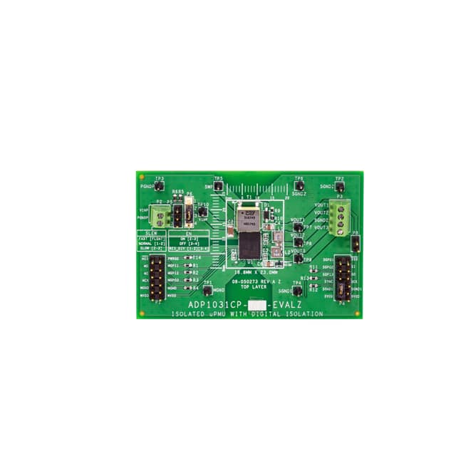
- Part No.:
- ADP1031ACPZ-3-R7
- Manufacturer:
- Analog Devices Inc.
- Category:
- Power Supply Controllers, Monitors
- Package:
- 41-VFQFN Exposed Pad, CSP
- Datasheet:
-
 ADP1031ACPZ-3-R7.pdf
- Description:
- ISO UPMU & DIGI 3.3VOUT2
- Quantity:
- Payment:

- Shipping:

Inventory:1,594
Please send an inquiry. Send us your inquiry, and we will respond immediately.
Product details
Overview
ADP1031ACPZ-3-R7 from Analog Devices is a three-channel isolated micropower management unit (PMU) integrating flyback, buck, and inverting dc-dc regulators with seven digital isolators. It delivers factory-programmed 3.3 V (VOUT2), adjustable −24 V to −5 V (VOUT3), and 6 V–28 V (VOUT1) outputs, supports 4.5 V–60 V input, and operates across −40°C to +125°C for industrial power and signal isolation in process control systems.
For engineers reviewing the ADP1031ACPZ-3-R7 datasheet, ADP1031ACPZ-3-R7 pinout, ADP1031ACPZ-3-R7 application, or ADP1031ACPZ-3-R7 equivalent, this page provides verified regulator output configurations, iCoupler® isolation timing specs, thermal shutdown thresholds, safety certification status, and domain-specific pin functions per Analog Devices Rev. A datasheet.
Technical Context
The ADP1031ACPZ-3-R7 implements three independent isolated regulators: a flyback (250 kHz default, 235–265 kHz range) with integrated 3 Ω FET and 300 mA current limit; a buck (125 kHz, 1 Ω NMOS/2.5 Ω PMOS FETs) delivering fixed 3.3 V at ±1.5% accuracy; and an inverting regulator (125 kHz, 1.45 Ω NMOS/2.2 Ω PMOS) generating −24 V to −5 V. All regulators use phase-shifted switching to reduce EMI.
Its seven digital isolators comprise four high-speed SPI channels (16.6 MHz, 7–15 ns propagation delay, 60–100 ps rms jitter) and three 100 kbps general-purpose GPIO channels (14 µs propagation delay), all based on iCoupler® chip-scale transformer technology with 565 VPEAK working insulation voltage and 2500 Vrms UL 1577 rating.
Key Specifications
| Parameter | Value and Actual Design Meaning |
|---|---|
| Input Voltage Range | 4.5 V to 60 V - supports wide industrial supply rails including 24 V DC and 48 V telecom systems. |
| VOUT2 Output | 3.3 V (factory-programmed) - fixed output for logic-level slave-side circuitry with ±1.5% accuracy over temperature. |
| VOUT3 Range | −24 V to −5 V - adjustable negative rail for analog front-ends, sensor biasing, or op-amp supplies. |
| Flyback Switch RON | 3 Ω - enables efficient power delivery up to 70 mA at 24 V while minimizing conduction loss. |
| SPI Isolation Propagation Delay | 7–15 ns - ensures deterministic timing for real-time control loops using isolated SPI interfaces. |
| Operating Junction Temp | −40°C to +125°C - qualified for harsh environments such as motor drives and PLC modules. |
| Insulation Rating | 2500 Vrms (1 min), VIORM = 565 VPEAK - meets IEC 61010-1 basic insulation requirements for field-to-control domain separation. |
| Total Output Power | 1720 mW - supports simultaneous operation of three isolated rails under full load (70 mA/7 mA/−0.3 mA). |
Pinout & Package
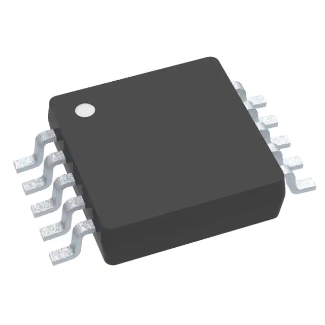
ADP1031ACPZ-3-R7 uses a 9 mm × 7 mm, 41-lead LFCSP package with three galvanically isolated domains: Field Power (VINP, SWP, PGNDP), Master (MVDD, MCK, MI, etc.), and Slave (SVDD1, VOUT1, FB1, SGPO1, etc.). Pins are grouped by domain and function; DNC pins (24, 25, 26) must remain unconnected.
| Pin/Terminal | Circuit Role | Design Meaning |
|---|---|---|
| 18 VOUT1 | Flyback output / Buck & Inverter input | Primary isolated positive rail (6–28 V); powers downstream buck/inverting regulators and external loads. |
| 15 VOUT2 | Buck regulator output | Fixed 3.3 V output for slave-side digital logic; requires no external feedback components. |
| 12 VOUT3 | Inverting regulator output | Negative rail (−24 V to −5 V); referenced to SGND2 and used for bipolar analog circuitry. |
| 11 FB3 | Inverting regulator feedback | Connects to resistor divider on VOUT3 to set output voltage; 0.8 V reference threshold. |
| 19 FB1 | Flyback regulator feedback | Connects to resistor divider on VOUT1; 0.8 V reference enables precise output programming. |
| 14 SYNC | External clock input | Accepts 350–750 kHz external oscillator to synchronize all three regulators and reduce EMI peaks. |
| 35 PWRGD | Power-good indicator | Open-drain output asserting high when all three regulators meet ±10% output tolerance windows. |
| 32 SLEW | Slew rate control | Selects slow (0.8 V threshold) or normal (2 V threshold) startup slew to limit inrush current. |
| 30 VINP | Main input supply | 4.5–60 V field-side input; feeds flyback controller and internal UVLO circuitry. |
| 29 SWP | Flyback switch node | Connects to primary side of 1:1 transformer; integrates 3 Ω power FET and 300 mA current limit. |
Key Features
| Feature | Design Value |
|---|---|
| Three isolated power rails | Simultaneous +6–28 V (VOUT1), +3.3 V (VOUT2), and −24 to −5 V (VOUT3) enable full analog/digital system isolation without external converters. |
| Phase-shifted triple-regulator architecture | Reduces peak EMI by staggering flyback (250 kHz), buck (125 kHz), and inverting (125 kHz) switching edges - critical for CISPR11 Class B compliance. |
| iCoupler® SPI isolation | Four 16.6 MHz, low-jitter (60–100 ps rms) channels provide deterministic, noise-immune communication between isolated domains for real-time control. |
| Integrated precision enable & power-good | EN pin with 1.135 V threshold and hysteresis ensures controlled startup; PWRGD asserts only when all three outputs stabilize within ±10%. |
| Transformer-agnostic design | 1:1 ratio transformer requirement simplifies magnetics selection and reduces BOM cost versus custom turns-ratio designs. |
| −40°C to +125°C junction rating | Validated operation across extended temperature range supports deployment in industrial enclosures without forced cooling. |
Applications
| Industrial Process Control | Data Acquisition Systems |
|---|---|
|
Use Scenario: Isolated analog input module acquiring 4–20 mA sensor signals in hazardous-area PLC backplanes. IC Role / Device Role / Timing Role: ADP1031ACPZ-3-R7 generates isolated ±15 V analog supply (via VOUT1/VOUT3) and 3.3 V digital rail (VOUT2) while isolating SPI commands to ADCs via its four high-speed channels. Use Value: Eliminates need for discrete isolated DC/DC converters and optocouplers, reducing board area by >40% and enabling single-chip power + data isolation. |
Use Scenario: High-precision 24-bit sigma-delta ADC subsystem capturing vibration and temperature data in rotating machinery. IC Role / Device Role / Timing Role: ADP1031ACPZ-3-R7 supplies clean, regulated ±5 V (VOUT1/VOUT3) for ADC reference and op-amps, and 3.3 V (VOUT2) for digital interface, with synchronized SPI isolation. Use Value: Phase-shifted regulators suppress switching noise coupling into sensitive analog paths, preserving ENOB in sub-100 µV measurement systems. |
| Programmable Logic Controllers | Motor Drive Control Boards |
|
Use Scenario: Modular I/O card with isolated digital inputs, relay drivers, and fieldbus communication (RS-485, CAN). IC Role / Device Role / Timing Role: ADP1031ACPZ-3-R7 powers isolated 24 V field-side inputs (VOUT1), 5 V logic (VOUT2), and −12 V gate bias (VOUT3), while isolating GPIO and SPI traffic. Use Value: Three dedicated isolated rails support mixed-voltage field interfaces without cross-domain interference or ground loop errors. |
Use Scenario: Gate driver stage for 3-phase IGBT inverters requiring isolated bootstrap and negative bias supplies. IC Role / Device Role / Timing Role: ADP1031ACPZ-3-R7 delivers isolated +15 V (VOUT1), +3.3 V (VOUT2), and −8 V (VOUT3) to gate drivers, with fast GPIO isolation for fault signaling. Use Value: Integrated inverting regulator eliminates external charge-pump ICs, reducing component count and improving reliability in high-vibration environments. |
Equivalent & Alternatives
The following parts are listed as comparable options for similar isolated power management applications.
| Alternative Part | Technical Difference | Application Difference | Selection Advice |
|---|---|---|---|
| ADP1032ACPZ-3-R7 | Same pinout and feature set but includes enhanced ESD protection (±8 kV HBM) and tighter VOUT2 initial accuracy (±1.0% vs. ±1.5%). | Preferred for new designs requiring higher robustness in electrostatic-prone manufacturing or field environments. | Select ADP1032ACPZ-3-R7 if ESD immunity and tighter output tolerance are critical; otherwise ADP1031ACPZ-3-R7 remains optimal for cost-sensitive deployments. |
| ISO1211DR | Dual-channel isolated power + data solution with only two regulators (5 V + 3.3 V) and five isolators; no negative rail or flyback integration. | Suitable for simpler isolated microcontroller interfaces but cannot replace ADP1031ACPZ-3-R7's triple-rail capability or −24 V to −5 V generation. | Choose ISO1211DR only for space-constrained, dual-rail applications where negative voltage is unnecessary and external inverter stages are acceptable. |
Compared with ADP1032ACPZ-3-R7 and ISO1211DR, the ADP1031ACPZ-3-R7 uniquely combines three isolated rails-including programmable negative output-with seven high-performance isolators in a single 9 mm × 7 mm package, making it the only solution capable of replacing discrete isolated DC/DC + digital isolator combinations in complex industrial subsystems.
Availability
ADP1031ACPZ-3-R7 is available at Aetrix Electronics and suitable for industrial automation, instrumentation, and data acquisition systems requiring stable component supply, long-term lifecycle assurance, and certified isolation performance.
Supply support for ADP1031ACPZ-3-R7 includes scheduled delivery planning, volume procurement assistance, BOM continuity management, traceable sourcing, and lifecycle availability coordination for OEM customers, industrial embedded developers, connected-device designers, and electronics production programs.
Manufacturer
Analog Devices, Inc. is a global leader in high-performance analog, mixed-signal, and digital signal processing semiconductors, serving industrial, automotive, communications, and healthcare markets.
The ADP1031ACPZ-3-R7 belongs to Analog Devices' isolated power management unit (PMU) product line, designed specifically to consolidate isolated power conversion and high-speed digital isolation into a single IC for rugged industrial control and measurement systems.
FAQ
What output voltage does ADP1031ACPZ-3-R7 deliver on VOUT2?
ADP1031ACPZ-3-R7 is factory-programmed to deliver a fixed 3.3 V output on VOUT2, with ±1.5% accuracy over −40°C to +125°C junction temperature and full load range. This value is permanently set during manufacturing and cannot be adjusted externally; it powers slave-side digital logic including SPI isolators and GPIO circuits.
How does ADP1031ACPZ-3-R7 achieve EMI reduction across its three regulators?
ADP1031ACPZ-3-R7 reduces electromagnetic interference by operating its flyback (250 kHz), buck (125 kHz), and inverting (125 kHz) regulators with phase-shifted switching edges. This staggers energy injection into shared magnetics and filtering networks, lowering peak spectral emissions to meet CISPR11 Class B radiated limits without additional shielding or complex layout constraints.
What safety certifications apply to ADP1031ACPZ-3-R7?
ADP1031ACPZ-3-R7 carries pending UL 1577 (2500 Vrms, 1 minute), CSA Component Acceptance Notice 5A, and VDE DIN V VDE 0884-10 (VIORM = 565 VPEAK) certifications. It meets IEC 61010-1 basic insulation requirements at 300 Vrms and supports 20-year lifetime at 0.1% failure rate under specified working voltage conditions.
Can ADP1031ACPZ-3-R7 generate a negative output voltage?
Yes, ADP1031ACPZ-3-R7 includes an integrated inverting dc-dc regulator that delivers an adjustable negative output (VOUT3) from −24 V to −5 V, referenced to SGND2. This rail is set via an external resistor divider on FB3 (0.8 V reference) and supports up to 15 mA load current with ±1.5% feedback accuracy.
What is the purpose of the SLEW pin on ADP1031ACPZ-3-R7?
The SLEW pin on ADP1031ACPZ-3-R7 selects startup slew rate: ≤0.8 V enables slow slew (reducing inrush current), while ≥2 V enables normal slew. It connects to VINP through a resistor divider or external control signal and must not float; a 100 kΩ pull-down to SGND2 is recommended per datasheet guidance.
ADP1031ACPZ-3-R7 Specifications
- Product attributes
- Attribute value
- Manufacturer:
- Analog Devices Inc.
- Series:
- -
- Package/Case:
- 41-VFQFN Exposed Pad, CSP
- Packaging:
- Tape & Reel (TR)
- Product Status:
- Active
- Programmable:
- Not Verified
- Applications:
- General Purpose
- Voltage - Input:
- 4.5V ~ 60V
- Voltage - Supply:
- 2.3V ~ 5.5V
- Current - Supply:
- -
- Operating Temperature:
- -40°C ~ 125°C (TJ)
- Grade:
- -
- Qualification:
- -
- Mounting Type:
- Surface Mount
- Supplier Device Package:
- 41-LFCSP (9x7)
ADP1031ACPZ-3-R7 FAQ
1.How can I place an order for ADP1031ACPZ-3-R7 through Aetrix?
Please submit a Request for Quotation (RFQ) for ADP1031ACPZ-3-R7 on Aetrix. Our sales agent will provide a competitive quotation and guide you through the order confirmation once you accept the terms.
2.Are the price and stock information for ADP1031ACPZ-3-R7 reliable?
The price and inventory of ADP1031ACPZ-3-R7 are updated periodically and may fluctuate due to market conditions. Stock and pricing data are typically refreshed every 24 hours. Quotation validity for ADP1031ACPZ-3-R7 is usually 5 days.
3.What payment methods are accepted for ADP1031ACPZ-3-R7?
We accept Wire Transfer, PayPal, Credit Card, Western Union, MoneyGram, and Escrow for ADP1031ACPZ-3-R7 transactions.
Note: Certain payment methods may incur a processing fee.
4.How is shipping managed for ADP1031ACPZ-3-R7?
ADP1031ACPZ-3-R7 orders can be shipped via leading logistics carriers, including DHL, UPS, FedEx, TNT, or Registered Mail.
Once your ADP1031ACPZ-3-R7 order is processed, you will receive an email with the shipment details and tracking number.
Note: Tracking information may take up to 24 hours to appear. Express delivery typically takes 3–5 business days.
5.How can I obtain technical support or documentation for ADP1031ACPZ-3-R7?
For technical support, including ADP1031ACPZ-3-R7 datasheets, pinout diagrams, or application guidance, please contact our engineering support team. They can provide detailed documentation and assistance for your ADP1031ACPZ-3-R7 requirements.
6.How does Aetrix verify that ADP1031ACPZ-3-R7 is sourced from the original manufacturer or authorized distributors?
All ADP1031ACPZ-3-R7 products on Aetrix are procured from qualified distributors and authorized channels. Our dedicated quality assurance team conducts strict verification, including traceability checks and, if necessary, third-party testing. This ensures that ADP1031ACPZ-3-R7 meets industry standards.
7.What is the process for return or replacement of ADP1031ACPZ-3-R7?
All ADP1031ACPZ-3-R7 units undergo pre-shipment inspection (PSI). If there is an issue with ADP1031ACPZ-3-R7, returns or replacements are accepted under the following conditions:
1.Quantity discrepancies, incorrect items, or visible external defects (such as breakage or corrosion), acknowledged by Aetrix.
2.The issue is reported within 90 days of delivery.
3.The ADP1031ACPZ-3-R7 part is unused and in its original packaging.
Return procedure for ADP1031ACPZ-3-R7:
1.Submit a request within 90 days.
2.Obtain a Return Material Authorization (RMA) from Aetrix.
ADP1031ACPZ-3-R7 Tags

-
UC3845AD8TR
Texas Instruments
-
UC2843AD8TR
Texas Instruments

-
LM3880MFX-1AE/NOPB
Texas Instruments
-
LM3880MFX-1AA/NOPB
Texas Instruments
-
INA234AIYBJR
Texas Instruments

-
INA700AYWFR
Texas Instruments
-
LM3880MF-1AE/NOPB
Texas Instruments
-
LM3880MF-1AA/NOPB
Texas Instruments
-
LM3881MM/NOPB
Texas Instruments
-
UCC2802DTR
Texas Instruments
-
NCP4305DMTTWG
onsemi
-
INA237AIDGSR
Texas Instruments
Tech Hub

A practical engineering guide to 3.3V and 5V logic compatibility, input thresholds, resistor dividers, translator ICs, MOSFET level shifting, I2C pull-ups, timing limits and power-sequencing risks.

The 74HC595 uses push-pull logic outputs, while the TPIC6B595 uses 50 V open-drain DMOS sinks for higher-power loads. This guide compares timing, current limits, 3.3 V interfacing, load wiring, thermal…

The 74HC595 converts serial data into eight stable parallel outputs. This guide covers pin functions, shift and storage timing, OE and MR behavior, drive-current limits, cascading, voltage compatibilit…

A technical comparison of level-sensitive latches and edge-triggered flip-flops, covering timing windows, setup and hold limits, master–slave operation, time borrowing, race-through, HDL inference and…

A D latch stores one bit while Enable controls when data can pass. This reference covers gate-level operation, truth tables, transparency, setup and hold timing, LE versus OE, common ICs and practical …

An SR latch stores one bit through cross-coupled feedback. This engineering reference covers NOR and NAND implementations, truth tables, forbidden-state recovery, gated operation, switch debouncing, fa…

Latch circuits retain one bit through feedback. This technical reference covers SR and D latches, truth tables, transparency, timing limits, latch-versus-flip-flop behavior, applications and common log…

An engineering guide to LED driver operation, constant-current and constant-voltage outputs, linear and switching topologies, dimming, IC selection, calculations, replacement compatibility, and fault c…

Operational amplifier guide covering op amp basics, feedback, ideal vs real op amps, common configurations, buffer circuits, offset, bias current, gain-bandwidth, slew rate, rail-to-rail limits and sel…

Jumper cables guide covering safe connection order, red and black clamp placement, final ground connection, cable gauge, length, clamp quality, copper vs CCA cables, jump starter comparison and battery…


