
 My Inquiry
 My Account


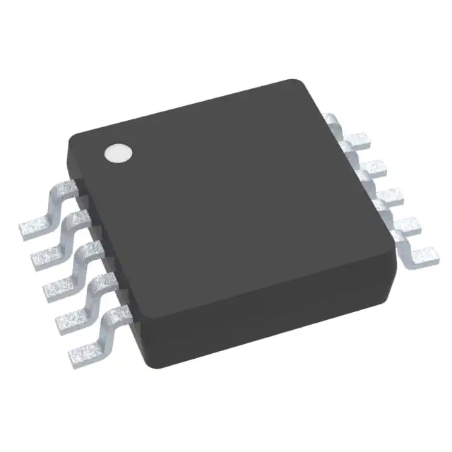
Analog Devices Inc. ADP1050ACPZ-R7
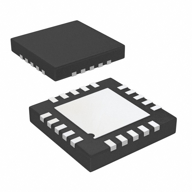
- Part No.:
- ADP1050ACPZ-R7
- Manufacturer:
- Analog Devices Inc.
- Category:
- Power Supply Controllers, Monitors
- Package:
- 20-WFQFN Exposed Pad, CSP
- Datasheet:
-
 ADP1050ACPZ-R7.pdf
- Description:
- IC DGTL PWR MGMT 20LFCSP
- Quantity:
- Payment:

- Shipping:

Inventory:885
Please send an inquiry. Send us your inquiry, and we will respond immediately.
Product details
Overview
ADP1050ACPZ-R7 from Analog Devices is a digital voltage mode controller for isolated DC-DC power supplies, featuring four 625 ps-resolution PWM outputs (OUTA, OUTB, SR1, SR2), PMBus interface compliance, and input voltage feedforward control. It operates from 3.0 V to 3.6 V supply, supports 49 kHz–625 kHz switching frequency, and delivers robust fault protection including conditional overvoltage, prebias startup, and pulse-skipping power saving - deployed in high-density server and telecom intermediate bus converters.
For engineers reviewing the ADP1050ACPZ-R7 datasheet, ADP1050ACPZ-R7 pinout, ADP1050ACPZ-R7 application, or ADP1050ACPZ-R7 equivalent, key selection criteria include its 20-lead 4 mm × 4 mm LFCSP package, integrated EEPROM programming, dual ADC paths (VS+/VS− and VF), real-time temperature monitoring via RTD, and programmable synchronous rectification timing for hard-switched topologies.
Technical Context
The ADP1050ACPZ-R7 implements voltage mode control with high-speed closed-loop input voltage feedforward using a dedicated 11-bit feedforward ADC (10 μs sampling period) and a separate 12-bit VS+ / VS− feedback ADC (10 ms update rate). Its flexible state machine architecture enables topology-specific PWM timing configuration across four independent outputs, with programmable rise/fall edge delays and 180° phase shift capability.
It integrates a 200 MHz PLL clock generator (set by 10 kΩ ±0.1% RES resistor), on-chip 2.6 V VCORE regulator (±0.15 V tolerance), and dual-path protection logic: analog comparators for CS1 OCP (65–105 ns latency) and digital flag-based fault responses (VOUT_OV_FAULT, VIN_UV_FAULT, OT_FAULT) triggered via PMBus-accessible registers.
Key Specifications
| Parameter | Value and Actual Design Meaning |
|---|---|
| Switching Frequency | 49 kHz to 625 kHz - supports wide-range optimization of magnetics size vs. efficiency in isolated flyback, forward, and full-bridge topologies. |
| PWM Resolution | 625 ps - enables fine-grained duty cycle control for precise regulation under fast transients and tight voltage tolerances. |
| Supply Voltage (VDD) | 3.0 V to 3.6 V - single-rail operation compatible with standard 3.3 V system rails; requires 2.2 μF decoupling capacitor at AGND. |
| Operating Temperature | −40°C to +125°C - qualified for industrial and telecom infrastructure environments with junction temperature up to 150°C. |
| Package | 20-lead LFCSP (4 mm × 4 mm) - thermally enhanced surface-mount package with exposed pad soldered to AGND plane for θJA = 37.05°C/W. |
| PMBus Compliance | Fully compliant with PMBus 1.2 - supports standardized commands for voltage/current/power readback, fault logging, and real-time register reconfiguration without firmware changes. |
| EEPROM Endurance | 10,000 write cycles at 85°C - stores calibrated compensation coefficients, startup sequences, and protection thresholds for standalone operation. |
Pinout & Package
The ADP1050ACPZ-R7 is housed in a 20-lead, 4 mm × 4 mm lead frame chip scale package (LFCSP) with an exposed thermal pad (EP) that must be soldered to the PCB AGND plane for optimal thermal performance and mechanical reliability.
| Pin/Terminal | Circuit Role | Design Meaning |
|---|---|---|
| OVP | Redundant overvoltage protection input | Differential comparator referenced to VS−; triggers VOUT_OV_FAULT flag with 61–85 ns latency and ±1.6% threshold accuracy over 0.75 V–1.5 V range. |
| VS− / VS+ | Differential output voltage sense inputs | High-accuracy 12-bit ADC path (±5% FSR error, 0–1.6 V range); used for closed-loop regulation and trimmable with ≤0.5% resistor dividers. |
| VF | Voltage feedforward input | 11-bit feedforward ADC (10 μs sampling) referenced to AGND; enables dynamic response improvement during line transients. |
| CS1 | Primary-side current sense input | 12-bit ADC + cycle-by-cycle OCP comparator (1.2 V or 0.25 V reference); 65–105 ns propagation delay for fast fault shutdown. |
| OUTA / OUTB / SR1 / SR2 | Programmable PWM logic outputs | Four independent 10 mA sink/source outputs with 3.5 ns rise / 1.5 ns fall time; support interleaving, phase shifting, and synchronous rectifier timing. |
| SYNI/FLGI | Synchronization input / external flag trigger | Accepts external clock (90–110% internal period match); enables multi-controller parallel operation with deterministic timing alignment. |
| SDA / SCL | PMBus/I²C bidirectional interface | Open-drain pins supporting 400 kHz Fast Mode; require pull-up resistors and provide full PMBus command set access including manufacturer-specific registers. |
| VCORE | On-chip 2.6 V regulator output | Stable 2.6 V ±0.15 V supply for internal logic; requires 330 nF decoupling capacitor and must not be used as external reference. |
| RTD | Thermistor temperature sense input | 12-bit ADC with factory-linearized NTC reading (±5°C accuracy from 25°C–125°C); supports 100 kΩ beta=4250 thermistors with 16.5 kΩ bias resistor. |
Key Features
| Feature | Design Value |
|---|---|
| Voltage mode control with input feedforward | Combines 12-bit slow/high-accuracy VS ADC and 11-bit fast feedforward ADC to improve transient response and reduce output ripple under line variation. |
| Four independent PWM outputs | OUTA/OUTB drive primary-side switches; SR1/SR2 control synchronous rectifiers with individually programmable dead time, phase offset, and soft-start sequencing. |
| Integrated EEPROM and GUI programming | Stores full configuration (compensation, protection thresholds, startup sequence); configured via free Analog Devices Digital Power Designer GUI without host MCU dependency. |
| Comprehensive fault protection | Hardware-level OVP (OVP pin), UVP (VF and VS paths), OCP (CS1 comparator), OTP (RTD path), and PGOOD monitoring - all reportable via PMBus flags and interrupt pins. |
| Prebias startup and pulse skipping | Enables reliable start-up into precharged output capacitors; pulse skipping reduces light-load quiescent current to <100 μA while maintaining regulation. |
Applications
| Server Intermediate Bus Converter | Telecom 48 V to 12 V Isolated PSU |
|---|---|
Use Scenario: High-efficiency 48 V to 12 V conversion in blade servers with strict space constraints and dynamic load steps. IC Role / Device Role / Timing Role: Digital controller managing active-clamp forward topology with synchronous rectification; regulates output using VS+/VS− feedback and adjusts switching frequency dynamically via PMBus. Use Value: Achieves >94% peak efficiency and <100 μs transient recovery using 625 ps PWM resolution and feedforward-enhanced loop response. | Use Scenario: Redundant 48 V input power modules in carrier-grade routers requiring hot-swap capability and parallel operation. IC Role / Device Role / Timing Role: Master/slave synchronized controller enabling N+1 redundancy; uses SYNI/FLGI for clock alignment and conditional OVP to isolate faulty units without system interruption. Use Value: Enables seamless failover with <10 μs synchronization jitter and automatic fault containment via PMBus-triggered shutdown sequences. |
| Industrial PLC Power Module | Network Switch Embedded PSU |
Use Scenario: Compact 24 V to 3.3 V/5 V isolated DC-DC module for programmable logic controllers operating in −40°C to +85°C ambient. IC Role / Device Role / Timing Role: Primary-side controller implementing half-bridge topology with prebias startup and RTD-based thermal derating; stores calibration in EEPROM for field-replaceable units. Use Value: Guarantees cold-start into precharged loads and extends lifetime via real-time junction temperature monitoring (±5°C accuracy up to 125°C). | Use Scenario: Multi-rail embedded power supply in 1U network switches requiring remote telemetry and firmware-upgradable protection settings. IC Role / Device Role / Timing Role: PMBus-configurable controller providing real-time IIN/VOUT/PIN/POUT readings, fault logs, and dynamic margining via SDA/SCL interface. Use Value: Eliminates need for external microcontrollers by delivering full power telemetry and configurable protection through standard PMBus commands. |
Equivalent & Alternatives
The following parts are listed as comparable options for similar digital power controller applications.
| Alternative Part | Technical Difference | Application Difference | Selection Advice |
|---|---|---|---|
| UCC28950RTJT | Analog voltage-mode controller with 4 PWM outputs; no integrated PMBus, EEPROM, or feedforward ADC; relies on external MCU for telemetry and configuration. | Lacks digital configurability and autonomous operation; suited for cost-sensitive designs where host MCU handles monitoring and updates. | Select when PMBus autonomy and GUI-based tuning are unnecessary and analog design familiarity is prioritized. |
| ISL68127IRAZ | Digital multiphase controller with integrated drivers; supports up to 7 phases; no isolated topology support; lacks VF feedforward and RTD sensing. | Optimized for VR12/IMVP8 CPU/GPU power delivery, not isolated dc-dc; targets high-current, low-voltage point-of-load rather than intermediate bus conversion. | Select only for non-isolated, multiphase POL applications; incompatible with transformer-coupled topologies requiring OVP/RTD/VS+/VS− isolation. |
Compared with UCC28950RTJT and ISL68127IRAZ, the ADP1050ACPZ-R7 uniquely combines isolated topology support, on-chip PMBus, feedforward-enhanced transient response, and autonomous EEPROM-based operation - making it the only option among the three qualified for high-availability, digitally managed, ultracompact isolated power modules.
Availability
ADP1050ACPZ-R7 is available at Aetrix Electronics and suitable for server power supplies, telecom infrastructure converters, and industrial PLC power modules requiring stable component supply, long-term lifecycle support, and guaranteed traceable sourcing.
Supply support for ADP1050ACPZ-R7 includes scheduled delivery planning, volume procurement assistance, BOM continuity management, traceable sourcing, and lifecycle availability coordination for OEM customers, industrial embedded developers, connected-device designers, and electronics production programs.
Manufacturer
Analog Devices is a global leader in high-performance analog, mixed-signal, and digital signal processing semiconductors, serving precision instrumentation, industrial automation, communications, and power management markets.
The ADP1050ACPZ-R7 belongs to Analog Devices' Digital Power Controller product line, designed specifically for high-density, high-efficiency isolated DC-DC conversion in data center, telecom, and industrial systems requiring programmable protection, telemetry, and autonomous operation.
FAQ
What is the primary function of the ADP1050ACPZ-R7 in a power supply design?
The ADP1050ACPZ-R7 serves as a fully programmable digital voltage mode controller for isolated DC-DC power supplies. It manages PWM generation, closed-loop regulation via VS+/VS− sensing, input voltage feedforward via the VF pin, primary-side current monitoring via CS1, and thermal monitoring via RTD - all coordinated through its internal state machine and stored in on-chip EEPROM. The ADP1050ACPZ-R7 eliminates the need for external microcontrollers in many applications by integrating PMBus communication, fault protection logic, and autonomous startup sequencing.
Does the ADP1050ACPZ-R7 support synchronous rectification, and how is it implemented?
Yes, the ADP1050ACPZ-R7 supports synchronous rectification using its SR1 and SR2 PWM outputs, which are functionally identical to OUTA and OUTB but optimized for secondary-side FET control. These outputs support programmable rising/falling edge timing, soft-start sequencing (via Register 0xFE08), and modulation limit constraints to prevent shoot-through. The ADP1050ACPZ-R7 allows independent configuration of SR timing relative to primary-side outputs, enabling precise dead-time control and adaptive gate drive for topologies like active-clamp forward and LLC with synchronous rectification.
How does the ADP1050ACPZ-R7 handle overvoltage protection, and what are the response characteristics?
The ADP1050ACPZ-R7 implements dual-path overvoltage protection: a fast analog comparator on the OVP pin (61–85 ns latency, ±1.6% threshold accuracy over 0.75 V–1.5 V) and a digital comparator on the VS+ path (10 ms update rate). When triggered, either path asserts the VOUT_OV_FAULT flag, initiates immediate PWM shutdown, and reports status via PMBus. The ADP1050ACPZ-R7 also supports conditional OVP - distinguishing between transient spikes and sustained faults - allowing safe shutdown only when multiple conditions align, preventing nuisance tripping in parallel power systems.
Can the ADP1050ACPZ-R7 operate without an external microcontroller, and what features enable this?
Yes, the ADP1050ACPZ-R7 is designed for standalone operation. Its on-chip 2.6 V VCORE regulator powers internal logic, the integrated EEPROM stores all configuration data (compensation, protection thresholds, startup parameters), and the PMBus interface allows initial programming and runtime monitoring without host intervention. The ADP1050ACPZ-R7 boots autonomously using EEPROM-loaded settings and maintains regulation, telemetry, and fault response entirely independently - verified by its use in embedded power modules where no external MCU is present.
What thermal sensing capability does the ADP1050ACPZ-R7 provide, and how accurate is it?
The ADP1050ACPZ-R7 provides high-accuracy junction temperature monitoring via its RTD pin, supporting NTC thermistors (100 kΩ, beta = 4250) with factory linearization. With default 46 μA bias current (Register 0xFE2D = 0xE6), it achieves ±5°C accuracy from 25°C to 100°C and ±7°C from 100°C to 125°C. Temperature readings are accessible via PMBus commands (READ_TEMPERATURE_1) and can trigger OT_FAULT for thermal shutdown. This capability is integral to the ADP1050ACPZ-R7's thermal derating and lifetime prediction features in high-reliability power systems.
ADP1050ACPZ-R7 Specifications
- Product attributes
- Attribute value
- Manufacturer:
- Analog Devices Inc.
- Series:
- -
- Package/Case:
- 20-WFQFN Exposed Pad, CSP
- Packaging:
- Tape & Reel (TR)
- Product Status:
- Active
- Programmable:
- Not Verified
- Applications:
- Power Supply Controller/Monitor
- Voltage - Input:
- 0V ~ 1.6V
- Voltage - Supply:
- 3V ~ 3.6V
- Current - Supply:
- 28.5 mA
- Operating Temperature:
- -40°C ~ 125°C
- Grade:
- -
- Qualification:
- -
- Mounting Type:
- Surface Mount
- Supplier Device Package:
- 20-LFCSP (4x4)
ADP1050ACPZ-R7 FAQ
1.How can I place an order for ADP1050ACPZ-R7 through Aetrix?
Please submit a Request for Quotation (RFQ) for ADP1050ACPZ-R7 on Aetrix. Our sales agent will provide a competitive quotation and guide you through the order confirmation once you accept the terms.
2.Are the price and stock information for ADP1050ACPZ-R7 reliable?
The price and inventory of ADP1050ACPZ-R7 are updated periodically and may fluctuate due to market conditions. Stock and pricing data are typically refreshed every 24 hours. Quotation validity for ADP1050ACPZ-R7 is usually 5 days.
3.What payment methods are accepted for ADP1050ACPZ-R7?
We accept Wire Transfer, PayPal, Credit Card, Western Union, MoneyGram, and Escrow for ADP1050ACPZ-R7 transactions.
Note: Certain payment methods may incur a processing fee.
4.How is shipping managed for ADP1050ACPZ-R7?
ADP1050ACPZ-R7 orders can be shipped via leading logistics carriers, including DHL, UPS, FedEx, TNT, or Registered Mail.
Once your ADP1050ACPZ-R7 order is processed, you will receive an email with the shipment details and tracking number.
Note: Tracking information may take up to 24 hours to appear. Express delivery typically takes 3–5 business days.
5.How can I obtain technical support or documentation for ADP1050ACPZ-R7?
For technical support, including ADP1050ACPZ-R7 datasheets, pinout diagrams, or application guidance, please contact our engineering support team. They can provide detailed documentation and assistance for your ADP1050ACPZ-R7 requirements.
6.How does Aetrix verify that ADP1050ACPZ-R7 is sourced from the original manufacturer or authorized distributors?
All ADP1050ACPZ-R7 products on Aetrix are procured from qualified distributors and authorized channels. Our dedicated quality assurance team conducts strict verification, including traceability checks and, if necessary, third-party testing. This ensures that ADP1050ACPZ-R7 meets industry standards.
7.What is the process for return or replacement of ADP1050ACPZ-R7?
All ADP1050ACPZ-R7 units undergo pre-shipment inspection (PSI). If there is an issue with ADP1050ACPZ-R7, returns or replacements are accepted under the following conditions:
1.Quantity discrepancies, incorrect items, or visible external defects (such as breakage or corrosion), acknowledged by Aetrix.
2.The issue is reported within 90 days of delivery.
3.The ADP1050ACPZ-R7 part is unused and in its original packaging.
Return procedure for ADP1050ACPZ-R7:
1.Submit a request within 90 days.
2.Obtain a Return Material Authorization (RMA) from Aetrix.
ADP1050ACPZ-R7 Tags

-
UC3845AD8TR
Texas Instruments
-
UC2843AD8TR
Texas Instruments

-
LM3880MFX-1AE/NOPB
Texas Instruments
-
LM3880MFX-1AA/NOPB
Texas Instruments
-
INA234AIYBJR
Texas Instruments

-
INA700AYWFR
Texas Instruments
-
LM3880MF-1AE/NOPB
Texas Instruments
-
LM3880MF-1AA/NOPB
Texas Instruments
-
LM3881MM/NOPB
Texas Instruments
-
UCC2802DTR
Texas Instruments
-
NCP4305DMTTWG
onsemi
-
INA237AIDGSR
Texas Instruments
Tech Hub

A practical engineering guide to 3.3V and 5V logic compatibility, input thresholds, resistor dividers, translator ICs, MOSFET level shifting, I2C pull-ups, timing limits and power-sequencing risks.

The 74HC595 uses push-pull logic outputs, while the TPIC6B595 uses 50 V open-drain DMOS sinks for higher-power loads. This guide compares timing, current limits, 3.3 V interfacing, load wiring, thermal…

The 74HC595 converts serial data into eight stable parallel outputs. This guide covers pin functions, shift and storage timing, OE and MR behavior, drive-current limits, cascading, voltage compatibilit…

A technical comparison of level-sensitive latches and edge-triggered flip-flops, covering timing windows, setup and hold limits, master–slave operation, time borrowing, race-through, HDL inference and…

A D latch stores one bit while Enable controls when data can pass. This reference covers gate-level operation, truth tables, transparency, setup and hold timing, LE versus OE, common ICs and practical …

An SR latch stores one bit through cross-coupled feedback. This engineering reference covers NOR and NAND implementations, truth tables, forbidden-state recovery, gated operation, switch debouncing, fa…

Latch circuits retain one bit through feedback. This technical reference covers SR and D latches, truth tables, transparency, timing limits, latch-versus-flip-flop behavior, applications and common log…

An engineering guide to LED driver operation, constant-current and constant-voltage outputs, linear and switching topologies, dimming, IC selection, calculations, replacement compatibility, and fault c…

Operational amplifier guide covering op amp basics, feedback, ideal vs real op amps, common configurations, buffer circuits, offset, bias current, gain-bandwidth, slew rate, rail-to-rail limits and sel…

Jumper cables guide covering safe connection order, red and black clamp placement, final ground connection, cable gauge, length, clamp quality, copper vs CCA cables, jump starter comparison and battery…


