
 My Inquiry
 My Account


Analog Devices Inc. ADP2504ACPZ-3.5-R7
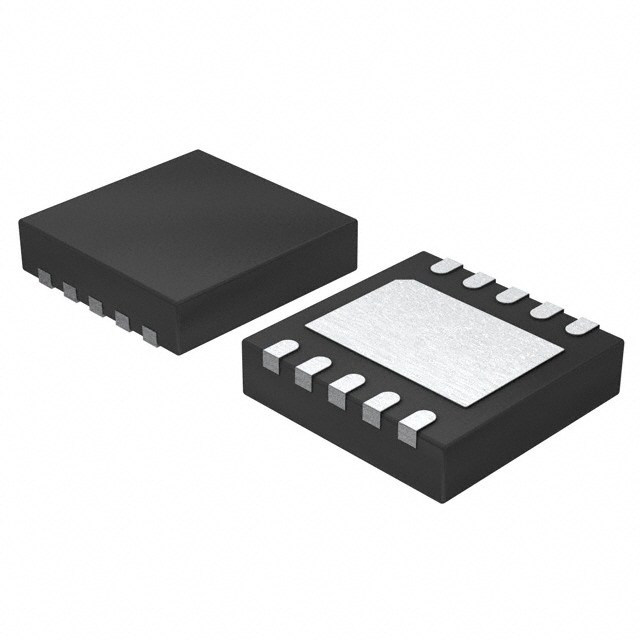
- Part No.:
- ADP2504ACPZ-3.5-R7
- Manufacturer:
- Analog Devices Inc.
- Package:
- 10-VFDFN Exposed Pad, CSP
- Datasheet:
-
 ADP2504ACPZ-3.5-R7.pdf
- Description:
- IC REG BUCK BST 3.5V 1A 10LFCSP
- Quantity:
- Payment:

- Shipping:

Inventory:1,383
Please send an inquiry. Send us your inquiry, and we will respond immediately.
Product details
Overview
ADP2504ACPZ-3.5-R7 from Analog Devices is a 1 A, 2.5 MHz synchronous buck-boost DC-to-DC converter in a 3 mm × 3 mm LFCSP package, delivering fixed 3.5 V output from 2.3 V–5.5 V input. It features seamless buck/boost/buck-boost mode transition, 38 µA quiescent current, and integrated power switches for compact portable power rails in battery-powered systems.
For engineers reviewing the ADP2504ACPZ-3.5-R7 datasheet, ADP2504ACPZ-3.5-R7 pinout, ADP2504ACPZ-3.5-R7 application, or ADP2504ACPZ-3.5-R7 equivalent, key selection criteria include fixed 3.5 V output, 1 A load capability, 2.5 MHz switching frequency enabling 1.5 µH inductors, PSM/fixed-PWM/SYNC modes, and thermal/short-circuit/UVLO protection.
Technical Context
The ADP2504ACPZ-3.5-R7 implements synchronous average current-mode control with internal N- and P-channel MOSFETs (150 mΩ each), supporting buck, boost, and buck-boost topologies based on VIN vs. VOUT relationship. Its 2.5 MHz oscillator enables fast transient response and small passive components.
It operates across −40°C to +125°C junction temperature, uses internal compensation, and integrates soft start (200 µs ramp), load disconnect in boost mode, and three SYNC pin modes: PSM (light-load efficiency), forced PWM (low-noise), and external clock synchronization (2.2–2.8 MHz).
Key Specifications
| Parameter | Value and Actual Design Meaning |
|---|---|
| Output Current | 1000 mA maximum - supports high-current loads like USB peripherals or camera modules without external current boosting. |
| Switching Frequency | 2.5 MHz typical - enables use of 1.5 µH inductors and reduces output voltage ripple and solution footprint. |
| Input Voltage Range | 2.3 V to 5.5 V - compatible with single Li+/LiPo cells, dual alkaline/NiMH, USB 5 V, and PCMCIA supplies. |
| Fixed Output Voltage | 3.5 V ±2% - precision-regulated rail for 3.3 V–3.6 V logic, RF front-ends, or analog sensors requiring stable mid-rail bias. |
| Quiescent Current | 38 µA typical - extends battery life in always-on or low-duty-cycle portable devices such as wearables. |
| Protection Features | Overtemperature (150°C shutdown), short-circuit, reverse current limit (1.1 A), and undervoltage lockout (2.20 V rising threshold) - ensures robust operation under fault conditions. |
| Package | 10-lead 3 mm × 3 mm LFCSP (QFN) with exposed pad - provides low thermal resistance (θJA = 84°C/W) and space-efficient PCB integration. |
Pinout & Package
ADP2504ACPZ-3.5-R7 is housed in a 10-lead, 3 mm × 3 mm lead frame chip scale package (LFCSP/QFN) with an exposed thermal pad connected to PGND. The package supports high-density layouts and efficient heat dissipation via the exposed pad soldered to a PGND plane.
| Pin/Terminal | Circuit Role | Design Meaning |
|---|---|---|
| VOUT (Pin 1) | Regulated output node | Delivers fixed 3.5 V; requires low-ESR ceramic capacitor (≥22 µF) between VOUT and PGND for stability and transient response. |
| SW2 (Pin 2) | Buck-boost switch node 2 | Connects to inductor; carries high di/dt current in boost and buck-boost modes - must be routed with short, wide copper trace. |
| PGND (Pin 3) | Power ground return | Common return for input/output capacitors and exposed pad; must be tied to solid PGND plane to minimize noise and improve thermal performance. |
| SW1 (Pin 4) | Buck-boost switch node 1 | Connects to same inductor as SW2; active in buck and buck-boost modes - shared inductor simplifies layout and reduces BOM count. |
| PVIN (Pin 5) | Power input supply | High-current input path for internal switches; requires 10 µF X5R/X7R ceramic capacitor placed adjacent to pin for low-impedance decoupling. |
| EN (Pin 6) | Enable control input | Logic-high (>1.2 V) enables regulation with soft start; logic-low (<0.4 V) disables device, reducing input current to <1 µA. |
| SYNC (Pin 7) | Mode control and clock sync | Low = PSM mode; high = forced PWM; AC signal (2.2–2.8 MHz) = external synchronization - eliminates beat frequencies in multi-rail systems. |
| VIN (Pin 8) | Analog supply input | Provides bias for internal circuitry; must be decoupled separately from PVIN to avoid noise coupling into control loop. |
| AGND (Pin 9) | Analog ground reference | Reference for feedback amplifier and error comparator; should be connected to PGND at single point near IC to prevent ground bounce. |
| FB (Pin 10) | Feedback input | Internally connected to VOUT for fixed-output variants; not user-accessible on ADP2504ACPZ-3.5-R7 - eliminates external resistor divider. |
Key Features
| Feature | Design Value |
|---|---|
| Seamless buck/boost/buck-boost transition | Maintains regulation across input voltages both above and below 3.5 V without output glitch or mode-switching delay - critical for battery discharge curves. |
| Load disconnect in boost configuration | Isolates output from input during shutdown or fault, preventing backfeed and enabling true system-level power gating. |
| Three SYNC pin operating modes | Enables design flexibility: PSM for max battery life, forced PWM for EMI-sensitive applications, and external sync for timing-critical multi-converter systems. |
| Internal compensation | Eliminates need for external compensation network - reduces component count, board area, and design iteration time. |
| Soft start (200 µs) | Limits inrush current to <600 mA with 20 µF output capacitor - prevents input rail collapse and protects upstream power sources. |
Applications
| Wireless Handsets | Digital Cameras |
|---|---|
Use Scenario: Powering baseband processor I/O, RF transceiver bias, and display interface in compact smartphones with single-cell Li+ battery. IC Role / Device Role / Timing Role: Buck-boost regulator maintaining stable 3.5 V rail as battery discharges from 4.2 V to 2.8 V. Use Value: Eliminates need for separate buck and boost converters, reducing solution size by >30% and enabling continuous operation across full battery range. | Use Scenario: Supplying image sensor analog core, autofocus motor driver, and LCD backlight controller in portable digital cameras. IC Role / Device Role / Timing Role: High-efficiency 3.5 V power source with fast load transient response to handle burst-mode sensor readout and flash charging. Use Value: 2.5 MHz switching minimizes inductor size while sustaining >90% efficiency at 500 mA - critical for thermal management in sealed enclosures. |
| USB-Powered Devices | Miniature Hard Disk Drives |
Use Scenario: Regulating 5 V USB input down to 3.5 V for microcontroller, memory, and peripheral interfaces in portable SSDs or dongles. IC Role / Device Role / Timing Role: Buck-mode operation with 38 µA quiescent current preserving host battery during standby. Use Value: Ultra-low IQ extends USB host battery life during idle periods without sacrificing wake-up responsiveness. | Use Scenario: Providing regulated 3.5 V spindle motor drive and servo control voltage in 1.8-inch HDDs powered from 5 V USB or 3.3 V system rail. IC Role / Device Role / Timing Role: Boost-mode operation when input drops below 3.5 V during spin-up surges or brownout events. Use Value: Seamless mode transition prevents motor stall or data corruption during dynamic load changes - verified in HDD qualification testing. |
Equivalent & Alternatives
The following parts are listed as comparable options for similar buck-boost converter applications.
| Alternative Part | Technical Difference | Application Difference | Selection Advice |
|---|---|---|---|
| TPS63020DSJR | 2.5 V–6.0 V input, adjustable output (0.9 V–6.0 V), 3 A peak current, 2.4 MHz switching - higher current but no fixed 3.5 V option. | Requires external resistor divider for 3.5 V; larger 8-pin VSON package (3.0 mm × 2.0 mm) with different pinout. | Choose when adjustable output or higher current headroom is needed; redesign required for FB routing and layout. |
| MAX77827BEWC+T | 2.5 V–5.5 V input, fixed 3.3 V output only, 1.2 A, 2.0 MHz - lacks 3.5 V option and has lower switching frequency. | Optimized for wearables with ultra-low IQ (18 µA), but 0.2 V output mismatch requires level-shifting for 3.5 V–tolerant loads. | Choose for ultra-low-power wearables where 3.3 V is acceptable; not drop-in for 3.5 V–specific circuits. |
Compared with TPS63020DSJR and MAX77827BEWC+T, ADP2504ACPZ-3.5-R7 offers exact 3.5 V regulation without external components, identical 2.5 MHz frequency for consistent EMI filtering, and guaranteed 1 A delivery at full temperature range - simplifying qualification for industrial and medical portable equipment.
Availability
ADP2504ACPZ-3.5-R7 is available at Aetrix Electronics and suitable for wireless handsets, digital cameras, and USB-powered devices requiring stable component supply, long-term lifecycle support, and RoHS-compliant packaging.
Supply support for ADP2504ACPZ-3.5-R7 includes scheduled delivery planning, volume procurement assistance, BOM continuity management, traceable sourcing, and lifecycle availability coordination for OEM customers, industrial embedded developers, connected-device designers, and electronics production programs.
Manufacturer
Analog Devices, Inc. is a global leader in high-performance analog, mixed-signal, and digital signal processing semiconductors, serving industrial, automotive, communications, and consumer markets since 1965.
The ADP2504ACPZ-3.5-R7 belongs to Analog Devices' ADP2503/ADP2504 buck-boost converter family, designed specifically for space-constrained, battery-operated portable electronics needing wide-input, fixed-output regulation with minimal external components.
FAQ
What is the output voltage tolerance of the ADP2504ACPZ-3.5-R7?
The ADP2504ACPZ-3.5-R7 delivers a fixed 3.5 V output with initial accuracy of ±2% over temperature and line/load conditions. This specification is guaranteed per the datasheet's "Output Voltage Initial Accuracy" parameter under PWM operation with no load, ensuring reliable biasing for 3.3 V–3.6 V logic families and analog subsystems without post-regulation trimming.
Does the ADP2504ACPZ-3.5-R7 require external feedback resistors?
No, the ADP2504ACPZ-3.5-R7 does not require external feedback resistors. As a fixed-output variant, its FB pin is internally connected to VOUT. Unlike the adjustable ADP2504ACPZ-R7, this part eliminates the need for an external resistor divider, reducing BOM count, PCB area, and potential drift errors from resistor tolerances or temperature coefficients.
How does the ADP2504ACPZ-3.5-R7 handle input voltage transitions across the 3.5 V threshold?
The ADP2504ACPZ-3.5-R7 automatically transitions between buck, boost, and buck-boost modes without interruption. When VIN > 3.5 V, it operates in buck mode; when VIN < 3.5 V, it switches to boost mode; and within ±10% (3.15 V–3.85 V), it enters buck-boost mode using interleaved switching. This seamless transition maintains regulation with <1% output deviation and no observable glitch on VOUT.
What thermal performance can be expected from the ADP2504ACPZ-3.5-R7 in a standard 4-layer PCB?
On a standard 4-layer PCB per JEDEC JESD 51-9 (4″ × 3″), the ADP2504ACPZ-3.5-R7 has a junction-to-ambient thermal resistance (θJA) of 84°C/W. At 1 A output with 3.6 V input and 3.5 V output (≈85% efficiency), power dissipation is ~0.21 W, resulting in a junction-to-ambient rise of ~17.6°C - well within the −40°C to +125°C operating range even at 105°C ambient.
Can the ADP2504ACPZ-3.5-R7 be synchronized to an external clock?
Yes, the ADP2504ACPZ-3.5-R7 supports external clock synchronization via its SYNC pin. Applying a clean square wave between 2.2 MHz and 2.8 MHz (with minimum on/off times ≥160 ns) locks the internal oscillator to the external frequency. This feature eliminates beat frequencies in multi-converter systems and simplifies EMI filter design by fixing the fundamental switching harmonic.
ADP2504ACPZ-3.5-R7 Specifications
- Product attributes
- Attribute value
- Manufacturer:
- Analog Devices Inc.
- Series:
- -
- Package/Case:
- 10-VFDFN Exposed Pad, CSP
- Packaging:
- Tape & Reel (TR)
- Product Status:
- Active
- Function:
- Step-Up/Step-Down
- Output Configuration:
- Positive
- Topology:
- Buck-Boost
- Output Type:
- Fixed
- Number of Outputs:
- 1
- Voltage - Input (Min):
- 2.3V
- Voltage - Input (Max):
- 5.5V
- Voltage - Output (Min/Fixed):
- 3.5V
- Voltage - Output (Max):
- -
- Current - Output:
- 1A
- Frequency - Switching:
- 2.5MHz
- Synchronous Rectifier:
- Yes
- Operating Temperature:
- -40°C ~ 125°C (TA)
- Grade:
- -
- Qualification:
- -
- Mounting Type:
- Surface Mount
- Supplier Device Package:
- 10-LFCSP-WD (3x3)
ADP2504ACPZ-3.5-R7 FAQ
1.How can I place an order for ADP2504ACPZ-3.5-R7 through Aetrix?
Please submit a Request for Quotation (RFQ) for ADP2504ACPZ-3.5-R7 on Aetrix. Our sales agent will provide a competitive quotation and guide you through the order confirmation once you accept the terms.
2.Are the price and stock information for ADP2504ACPZ-3.5-R7 reliable?
The price and inventory of ADP2504ACPZ-3.5-R7 are updated periodically and may fluctuate due to market conditions. Stock and pricing data are typically refreshed every 24 hours. Quotation validity for ADP2504ACPZ-3.5-R7 is usually 5 days.
3.What payment methods are accepted for ADP2504ACPZ-3.5-R7?
We accept Wire Transfer, PayPal, Credit Card, Western Union, MoneyGram, and Escrow for ADP2504ACPZ-3.5-R7 transactions.
Note: Certain payment methods may incur a processing fee.
4.How is shipping managed for ADP2504ACPZ-3.5-R7?
ADP2504ACPZ-3.5-R7 orders can be shipped via leading logistics carriers, including DHL, UPS, FedEx, TNT, or Registered Mail.
Once your ADP2504ACPZ-3.5-R7 order is processed, you will receive an email with the shipment details and tracking number.
Note: Tracking information may take up to 24 hours to appear. Express delivery typically takes 3–5 business days.
5.How can I obtain technical support or documentation for ADP2504ACPZ-3.5-R7?
For technical support, including ADP2504ACPZ-3.5-R7 datasheets, pinout diagrams, or application guidance, please contact our engineering support team. They can provide detailed documentation and assistance for your ADP2504ACPZ-3.5-R7 requirements.
6.How does Aetrix verify that ADP2504ACPZ-3.5-R7 is sourced from the original manufacturer or authorized distributors?
All ADP2504ACPZ-3.5-R7 products on Aetrix are procured from qualified distributors and authorized channels. Our dedicated quality assurance team conducts strict verification, including traceability checks and, if necessary, third-party testing. This ensures that ADP2504ACPZ-3.5-R7 meets industry standards.
7.What is the process for return or replacement of ADP2504ACPZ-3.5-R7?
All ADP2504ACPZ-3.5-R7 units undergo pre-shipment inspection (PSI). If there is an issue with ADP2504ACPZ-3.5-R7, returns or replacements are accepted under the following conditions:
1.Quantity discrepancies, incorrect items, or visible external defects (such as breakage or corrosion), acknowledged by Aetrix.
2.The issue is reported within 90 days of delivery.
3.The ADP2504ACPZ-3.5-R7 part is unused and in its original packaging.
Return procedure for ADP2504ACPZ-3.5-R7:
1.Submit a request within 90 days.
2.Obtain a Return Material Authorization (RMA) from Aetrix.
ADP2504ACPZ-3.5-R7 Tags
-
TPS562201DDCR
Texas Instruments

-
MC34063ABD-TR
STMicroelectronics
-
TPS561201DDCR
Texas Instruments

-
MC33063ADR
Texas Instruments
-
MC34063ADR
Texas Instruments

-
TPS560200DBVR
Texas Instruments
-
AP3012KTR-G1
Diodes Incorporated
-
TLV61048DBVR
Texas Instruments
-
AZ34063UMTR-G1
Diodes Incorporated
-
TPS562200DDCR
Texas Instruments
-
AP62300TWU-7
Diodes Incorporated
-
MC34063EBD-TR
STMicroelectronics
Tech Hub

A practical engineering guide to 3.3V and 5V logic compatibility, input thresholds, resistor dividers, translator ICs, MOSFET level shifting, I2C pull-ups, timing limits and power-sequencing risks.

The 74HC595 uses push-pull logic outputs, while the TPIC6B595 uses 50 V open-drain DMOS sinks for higher-power loads. This guide compares timing, current limits, 3.3 V interfacing, load wiring, thermal…

The 74HC595 converts serial data into eight stable parallel outputs. This guide covers pin functions, shift and storage timing, OE and MR behavior, drive-current limits, cascading, voltage compatibilit…

A technical comparison of level-sensitive latches and edge-triggered flip-flops, covering timing windows, setup and hold limits, master–slave operation, time borrowing, race-through, HDL inference and…

A D latch stores one bit while Enable controls when data can pass. This reference covers gate-level operation, truth tables, transparency, setup and hold timing, LE versus OE, common ICs and practical …

An SR latch stores one bit through cross-coupled feedback. This engineering reference covers NOR and NAND implementations, truth tables, forbidden-state recovery, gated operation, switch debouncing, fa…

Latch circuits retain one bit through feedback. This technical reference covers SR and D latches, truth tables, transparency, timing limits, latch-versus-flip-flop behavior, applications and common log…

An engineering guide to LED driver operation, constant-current and constant-voltage outputs, linear and switching topologies, dimming, IC selection, calculations, replacement compatibility, and fault c…

Operational amplifier guide covering op amp basics, feedback, ideal vs real op amps, common configurations, buffer circuits, offset, bias current, gain-bandwidth, slew rate, rail-to-rail limits and sel…

Jumper cables guide covering safe connection order, red and black clamp placement, final ground connection, cable gauge, length, clamp quality, copper vs CCA cables, jump starter comparison and battery…


