
 My Inquiry
 My Account


Analog Devices Inc. ADP5061ACBZ-4-R7
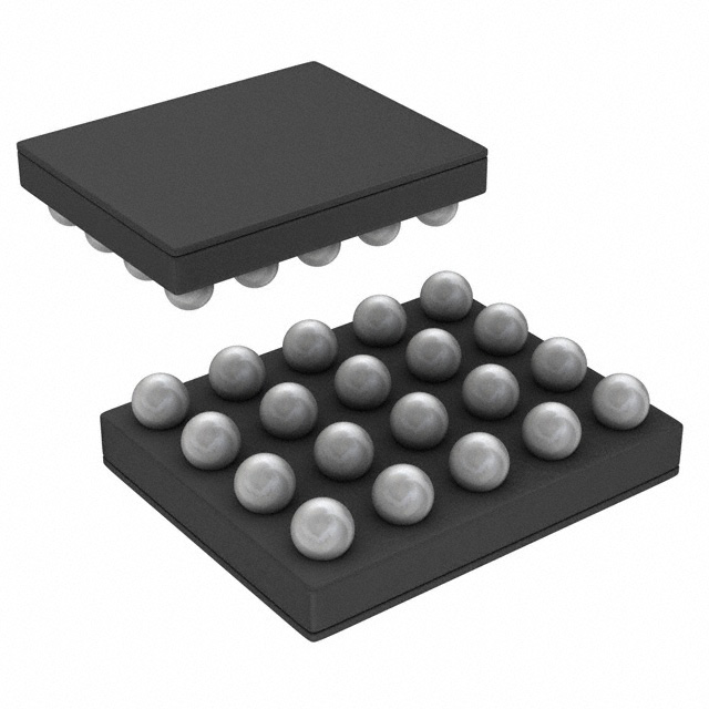
- Part No.:
- ADP5061ACBZ-4-R7
- Manufacturer:
- Analog Devices Inc.
- Category:
- Battery Chargers
- Package:
- 20-WFBGA, WLCSP
- Datasheet:
-
 ADP5061ACBZ-4-R7.pdf
- Description:
- IC BATT CHG LI-ION 1CELL 20WLCSP
- Quantity:
- Payment:

- Shipping:

Inventory:8,975
Please send an inquiry. Send us your inquiry, and we will respond immediately.
Product details
Overview
ADP5061ACBZ-4-R7 from Analog Devices is a tiny, I²C-programmable linear battery charger IC with integrated power path management and USB Battery Charging Specification 1.2 compliance. It delivers up to 2.1 A system supply current in LDO mode, supports 4.0 V–6.7 V input voltage range with ±20 V tolerance, and features factory-programmable DIG_IO2/DIG_IO3 pins for charging enable/disable control specific to this variant.
For engineers reviewing the ADP5061ACBZ-4-R7 datasheet, ADP5061ACBZ-4-R7 pinout, ADP5061ACBZ-4-R7 application, or ADP5061ACBZ-4-R7 equivalent, key selection criteria include its 2.6 mm × 2.0 mm WLCSP package, JEITA-compliant temperature-aware charging, 30 mΩ battery isolation FET, programmable fast-charge current (750 mA typ), and dual-mode operation (charger + system LDO) with SYS_EN flag for battery-level–gated system startup.
Technical Context
The ADP5061ACBZ-4-R7 implements a fully integrated linear charging architecture with three independent VIN inputs (VIN1/VIN2/VIN3), three ISO_S/ISO_B power path channels, and factory-configured DIG_IO2/DIG_IO3 logic for charging enable/disable - distinguishing it from -2-R7 (DIG_IO2 disables IC1) and -5-R7 (DIG_IO3 is interrupt output). Its internal 30 mΩ isolation FET enables system power-up from USB even with dead or absent battery.
Charging behavior is governed by JEITA 1 or JEITA 2 profiles (selectable via I²C), with cold/hot thresholds at 0°C/60°C and programmable termination voltage (4.200 V nominal). Thermal regulation limits junction temperature to 115°C during isothermal charging, with shutdown at 140°C and early warning at 130°C.
Key Specifications
| Parameter | Value and Actual Design Meaning |
|---|---|
| Input Voltage Range | 4.0 V to 6.7 V operating; −0.5 V to +20 V tolerant - enables robust USB VBUS interface without external overvoltage protection |
| Max System Output Current | 2.1 A in LDO mode - powers system directly from USB input while charging battery |
| Battery Isolation FET RDS(ON) | 30 mΩ typical - minimizes voltage drop between battery and system rail, enabling immediate system boot under dead-battery condition |
| Fast Charge Current | 750 mA typical (±30 mA accuracy) - programmable via I²C register ICHG[4:0], guaranteed across −40°C to +115°C |
| Termination Voltage Accuracy | ±0.25% at 25°C (±0.89% over 0°C–115°C) - ensures precise Li-ion full-charge cutoff at 4.200 V on BAT_SNS |
| Package | 20-ball WLCSP, 2.6 mm × 2.0 mm, 0.5 mm pitch - ultra-compact footprint for space-constrained portable devices |
| I²C Interface | 400 kHz standard-mode compatible - enables full configuration of charge parameters, JEITA profile, and safety timers |
Pinout & Package
ADP5061ACBZ-4-R7 uses a 20-ball Wafer-Level Chip-Scale Package (WLCSP) with 0.5 mm pitch, measuring 2.6 mm × 2.0 mm. Ball-side-down top view places ILED at A4, AGND at B1, and DIG_IO3 (charging enable) at B4.
| Pin/Terminal | Circuit Role | Design Meaning |
|---|---|---|
| ISO_S1/ISO_S2/ISO_S3 | System Supply Output | High-current outputs feeding regulated system rail; connect to bulk capacitors (≥20 μF) for LDO stability |
| VIN1/VIN2/VIN3 | USB VBUS Input | Parallel-connected 20 V-tolerant inputs accepting wall/car/USB host power; require ≥4 μF CVIN |
| ISO_B1/ISO_B2/ISO_B3 | Battery Supply Input | Inputs to battery-side isolation FET; sense battery voltage via BAT_SNS and regulate charge current |
| DIG_IO3 | Charging Enable Control | For ADP5061ACBZ-4-R7: high = enable charging; low/high-Z = disable - overrides I²C register when not reset by VIN disconnect |
| BAT_SNS | Battery Voltage Sense | High-impedance analog input monitoring battery voltage for charge state, termination, and JEITA temperature profiling |
| SYS_EN | System Enable Flag | Open-drain output asserting when battery reaches VWEAK (2.89–3.11 V); used to gate system power-on sequencing |
Key Features
| Feature | Design Value |
|---|---|
| USB BC 1.2 & USB 3.0 Compliance | Automatically adapts input current limit (100 mA to 1500 mA) based on USB source detection - eliminates need for external USB ID chip in basic implementations |
| Power Path Management | Integrated 30 mΩ isolation FET allows simultaneous battery charging and system operation - enables instant system boot even with 0 V battery |
| JEITA Temperature Profiling | Configurable cold/hot thresholds (0°C/60°C) and programmable VTRM reduction (−100 mV in warm zone) - prevents Li-ion thermal stress during charging |
| Factory-Programmed DIG_IO Logic | DIG_IO3 hardwired as charging enable for ADP5061ACBZ-4-R7 - simplifies board design by eliminating I²C initialization dependency for basic enable/disable control |
| Thermal Regulation & Safety | Three-tier thermal response: isothermal charging at 115°C, early warning at 130°C, shutdown at 140°C - prevents thermal runaway under sustained high-power conditions |
Applications
| Mobile Phones | Digital Still Cameras |
|---|---|
Use Scenario: Compact smartphone requiring USB-powered boot and battery charging from single mini-USB port. IC Role / Device Role / Timing Role: Linear charger + system LDO with power path; manages battery charge state while powering baseband processor and display. Use Value: Enables immediate system wake-up on USB insertion (via SYS_EN flag) and maintains stable 4.3 V system rail during charging - no brownout during high-current bursts. |
Use Scenario: High-resolution digital camera needing rapid power-up and reliable charging from USB or AC adapter. IC Role / Device Role / Timing Role: Dual-role power manager: supplies 2.1 A system load in LDO mode while delivering 750 mA CC charge current to single-cell Li-ion pack. Use Value: 30 mΩ isolation FET ensures <100 mV dropout at 1 A system load - preserves headroom for image sensor and flash LED drivers. |
| Portable Medical Devices | PDAs & GPS Navigation Units |
Use Scenario: FDA-classified handheld diagnostic tool requiring fail-safe charging and battery health monitoring. IC Role / Device Role / Timing Role: JEITA-compliant charger with thermistor-based temperature sensing (THR pin) and precise 4.200 V termination voltage. Use Value: ±0.25% VTRM accuracy at 25°C and cold/hot cutoffs prevent overcharge/undercharge - critical for battery longevity and regulatory compliance. |
Use Scenario: Legacy PDA or automotive GPS unit with mini-USB connectivity and tight PCB area constraints. IC Role / Device Role / Timing Role: Ultra-small (2.6 mm × 2.0 mm) WLCSP charger managing both system power and battery conditioning. Use Value: Factory-programmed DIG_IO3 eliminates I²C firmware dependency for charging enable - reduces BOM count and boot-time complexity. |
Equivalent & Alternatives
The following parts are listed as comparable options for similar linear battery charger applications.
| Alternative Part | Technical Difference | Application Difference | Selection Advice |
|---|---|---|---|
| BQ24075RGTR | 5-pin SOT-23 package; fixed 4.2 V termination; no JEITA support; 1.5 A max system current | Lacks thermal profiling and USB BC 1.2 auto-detection - requires external USB ID circuitry for compliant charging | Choose for cost-sensitive, non-JEITA designs where 1.5 A system current suffices and board space permits larger SOT-23 footprint |
| MAX1555 | 8-pin μMAX package; 500 mA max charge current; no I²C; fixed 4.2 V termination; no power path | No system LDO mode or battery isolation - cannot power system while charging; no thermal regulation beyond shutdown | Choose only for simple, low-current (≤500 mA) applications where system must be off during charging and JEITA compliance is unnecessary |
Compared with BQ24075RGTR and MAX1555, ADP5061ACBZ-4-R7 provides superior integration: USB BC 1.2 auto-detection avoids external ID chips, JEITA 1/2 support enables safe wide-temperature charging, and 2.1 A LDO mode with 30 mΩ FET allows true power-path operation - making it optimal for compact, feature-rich portable electronics.
Availability
ADP5061ACBZ-4-R7 is available at Aetrix Electronics and suitable for mobile phones, digital cameras, portable medical devices, and PDAs requiring stable component supply, JEITA-compliant charging, and ultra-compact power management integration.
Supply support for ADP5061ACBZ-4-R7 includes scheduled delivery planning, volume procurement assistance, BOM continuity management, traceable sourcing, and lifecycle availability coordination for OEM customers, industrial embedded developers, connected-device designers, and electronics production programs.
Manufacturer
Analog Devices is a global leader in high-performance analog, mixed-signal, and digital signal processing semiconductors, serving precision instrumentation, industrial automation, communications, and healthcare markets.
The ADP5061 product line delivers highly integrated, USB-compliant linear battery chargers with power path and JEITA temperature management - designed specifically for space-constrained, battery-powered portable electronics demanding robust USB charging and system reliability.
FAQ
What is the primary function of the DIG_IO3 pin on the ADP5061ACBZ-4-R7?
On the ADP5061ACBZ-4-R7, DIG_IO3 serves as the dedicated charging enable control pin. When driven high, it enables battery charging; when low or high-impedance, it disables charging - overriding I²C register settings until VIN is cycled. This hardware-level control simplifies system power sequencing and ensures fail-safe disable capability independent of firmware initialization.
How does the ADP5061ACBZ-4-R7 handle USB compliance without an external USB ID chip?
The ADP5061ACBZ-4-R7 supports USB Battery Charging Specification 1.2 natively through its programmable input current limit logic. While it relies on an external USB detection chip to identify source type (SDP/CDP/DCP), its I²C interface allows direct configuration of appropriate current limits (100 mA, 500 mA, 900 mA, or 1500 mA) - eliminating the need for additional logic to translate ID signals into charge control.
What is the significance of the 30 mΩ battery isolation FET in the ADP5061ACBZ-4-R7?
The 30 mΩ typical RDS(ON) of the internal battery isolation FET in the ADP5061ACBZ-4-R7 enables efficient power path operation: it allows the system to draw up to 2.1 A directly from VIN while simultaneously charging the battery, and permits immediate system boot even with a completely discharged (0 V) battery - a critical capability for consumer electronics requiring instant responsiveness on USB connection.
Can the ADP5061ACBZ-4-R7 operate safely in high-temperature environments like automotive cabins?
The ADP5061ACBZ-4-R7 incorporates multi-stage thermal protection: isothermal charging begins at 115°C, early warning triggers at 130°C, and thermal shutdown occurs at 140°C. While its specified operating junction range is −40°C to +125°C, sustained ambient temperatures above 85°C require careful PCB thermal design (e.g., copper pour, thermal vias) - it is qualified for industrial, not automotive AEC-Q100, applications.
What are the key differences between ADP5061ACBZ-4-R7 and ADP5061ACBZ-2-R7?
The ADP5061ACBZ-4-R7 and ADP5061ACBZ-2-R7 share identical core functionality but differ in factory-programmed DIG_IO pin mapping: on the -4-R7, DIG_IO3 is configured as charging enable; on the -2-R7, DIG_IO2 is configured as IC1 disable. Both variants use the same WLCSP package and support identical I²C programming, JEITA profiles, and electrical specifications - the distinction is purely in default GPIO behavior.
ADP5061ACBZ-4-R7 Specifications
- Product attributes
- Attribute value
- Manufacturer:
- Analog Devices Inc.
- Series:
- -
- Package/Case:
- 20-WFBGA, WLCSP
- Packaging:
- Tape & Reel (TR)
- Product Status:
- Active
- Battery Chemistry:
- Lithium Ion
- Number of Cells:
- 1
- Current - Charging:
- Constant - Programmable
- Programmable Features:
- -
- Fault Protection:
- -
- Charge Current - Max:
- 1.3A
- Battery Pack Voltage:
- 4.3V
- Voltage - Supply (Max):
- 6.7V
- Interface:
- I2C, USB
- Operating Temperature:
- -40°C ~ 125°C (TJ)
- Grade:
- -
- Qualification:
- -
- Mounting Type:
- Surface Mount
- Supplier Device Package:
- 20-WLCSP (2x2.6)
ADP5061ACBZ-4-R7 FAQ
1.How can I place an order for ADP5061ACBZ-4-R7 through Aetrix?
Please submit a Request for Quotation (RFQ) for ADP5061ACBZ-4-R7 on Aetrix. Our sales agent will provide a competitive quotation and guide you through the order confirmation once you accept the terms.
2.Are the price and stock information for ADP5061ACBZ-4-R7 reliable?
The price and inventory of ADP5061ACBZ-4-R7 are updated periodically and may fluctuate due to market conditions. Stock and pricing data are typically refreshed every 24 hours. Quotation validity for ADP5061ACBZ-4-R7 is usually 5 days.
3.What payment methods are accepted for ADP5061ACBZ-4-R7?
We accept Wire Transfer, PayPal, Credit Card, Western Union, MoneyGram, and Escrow for ADP5061ACBZ-4-R7 transactions.
Note: Certain payment methods may incur a processing fee.
4.How is shipping managed for ADP5061ACBZ-4-R7?
ADP5061ACBZ-4-R7 orders can be shipped via leading logistics carriers, including DHL, UPS, FedEx, TNT, or Registered Mail.
Once your ADP5061ACBZ-4-R7 order is processed, you will receive an email with the shipment details and tracking number.
Note: Tracking information may take up to 24 hours to appear. Express delivery typically takes 3–5 business days.
5.How can I obtain technical support or documentation for ADP5061ACBZ-4-R7?
For technical support, including ADP5061ACBZ-4-R7 datasheets, pinout diagrams, or application guidance, please contact our engineering support team. They can provide detailed documentation and assistance for your ADP5061ACBZ-4-R7 requirements.
6.How does Aetrix verify that ADP5061ACBZ-4-R7 is sourced from the original manufacturer or authorized distributors?
All ADP5061ACBZ-4-R7 products on Aetrix are procured from qualified distributors and authorized channels. Our dedicated quality assurance team conducts strict verification, including traceability checks and, if necessary, third-party testing. This ensures that ADP5061ACBZ-4-R7 meets industry standards.
7.What is the process for return or replacement of ADP5061ACBZ-4-R7?
All ADP5061ACBZ-4-R7 units undergo pre-shipment inspection (PSI). If there is an issue with ADP5061ACBZ-4-R7, returns or replacements are accepted under the following conditions:
1.Quantity discrepancies, incorrect items, or visible external defects (such as breakage or corrosion), acknowledged by Aetrix.
2.The issue is reported within 90 days of delivery.
3.The ADP5061ACBZ-4-R7 part is unused and in its original packaging.
Return procedure for ADP5061ACBZ-4-R7:
1.Submit a request within 90 days.
2.Obtain a Return Material Authorization (RMA) from Aetrix.
ADP5061ACBZ-4-R7 Tags

-
BQ21040DBVR
Texas Instruments

-
MCP73812T-420I/OT
Microchip Technology
-
MCP73831T-2ACI/OT
Microchip Technology
-
MCP73832T-2ACI/OT
Microchip Technology
-
MCP73831T-2DCI/OT
Microchip Technology
-
MCP73832T-2DCI/OT
Microchip Technology
-
MCP73831T-2ATI/OT
Microchip Technology
-
MCP73832T-2ATI/OT
Microchip Technology
-
MCP73831T-5ACI/OT
Microchip Technology

-
MCP73832T-2ACI/MC
Microchip Technology
-
MCP73831T-2ACI/MC
Microchip Technology
-
MCP73831T-2ATI/MC
Microchip Technology
Tech Hub

A practical engineering guide to 3.3V and 5V logic compatibility, input thresholds, resistor dividers, translator ICs, MOSFET level shifting, I2C pull-ups, timing limits and power-sequencing risks.

The 74HC595 uses push-pull logic outputs, while the TPIC6B595 uses 50 V open-drain DMOS sinks for higher-power loads. This guide compares timing, current limits, 3.3 V interfacing, load wiring, thermal…

The 74HC595 converts serial data into eight stable parallel outputs. This guide covers pin functions, shift and storage timing, OE and MR behavior, drive-current limits, cascading, voltage compatibilit…

A technical comparison of level-sensitive latches and edge-triggered flip-flops, covering timing windows, setup and hold limits, master–slave operation, time borrowing, race-through, HDL inference and…

A D latch stores one bit while Enable controls when data can pass. This reference covers gate-level operation, truth tables, transparency, setup and hold timing, LE versus OE, common ICs and practical …

An SR latch stores one bit through cross-coupled feedback. This engineering reference covers NOR and NAND implementations, truth tables, forbidden-state recovery, gated operation, switch debouncing, fa…

Latch circuits retain one bit through feedback. This technical reference covers SR and D latches, truth tables, transparency, timing limits, latch-versus-flip-flop behavior, applications and common log…

An engineering guide to LED driver operation, constant-current and constant-voltage outputs, linear and switching topologies, dimming, IC selection, calculations, replacement compatibility, and fault c…

Operational amplifier guide covering op amp basics, feedback, ideal vs real op amps, common configurations, buffer circuits, offset, bias current, gain-bandwidth, slew rate, rail-to-rail limits and sel…

Jumper cables guide covering safe connection order, red and black clamp placement, final ground connection, cable gauge, length, clamp quality, copper vs CCA cables, jump starter comparison and battery…


