
 My Inquiry
 My Account


Analog Devices Inc. ADP5062ACPZ-2-R7
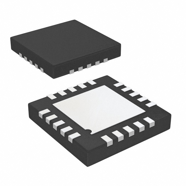
- Part No.:
- ADP5062ACPZ-2-R7
- Manufacturer:
- Analog Devices Inc.
- Category:
- Battery Chargers
- Package:
- 20-WFQFN Exposed Pad, CSP
- Datasheet:
-
 ADP5062ACPZ-2-R7.pdf
- Description:
- IC BATT CHG LI-ION 1CELL 20LFCSP
- Quantity:
- Payment:

- Shipping:

Inventory:3,898
Please send an inquiry. Send us your inquiry, and we will respond immediately.
Product details
Overview
ADP5062ACPZ-2-R7 from Analog Devices is a fully programmable linear Li-ion battery charger with Power Path management, USB 3.0 and USB Battery Charging Specification 1.2 compliance, 4 mm × 4 mm LFCSP package, 750 mA fast charge current (typ), and integrated 54 mΩ battery isolation FET - used in portable medical devices and mobile phones to enable system power-up from dead-battery conditions.
For engineers reviewing the ADP5062ACPZ-2-R7 datasheet, ADP5062ACPZ-2-R7 pinout, ADP5062ACPZ-2-R7 application, or ADP5062ACPZ-2-R7 equivalent, key selection criteria include USB-compliant input current limiting (100–1500 mA), JEITA-compliant temperature-based charging (0°C–60°C), thermal regulation (115°C isothermal limit), and I²C + GPIO configurability for flexible system integration.
Technical Context
The ADP5062ACPZ-2-R7 implements dual-path power management: a high-voltage blocking LDO FET (RDS(ON) = 330 mΩ) delivers up to 2.1 A system supply, while a low-RDS(ON) (54 mΩ typ) battery isolation FET enables simultaneous battery charging and system operation. It supports three distinct charging phases - trickle (20 mA typ), weak, and fast (750 mA typ) - with voltage thresholds at VTRK_DEAD = 2.5 V and VWEAK = 3.0 V.
Thermal control uses isothermal regulation (TLIM = 115°C), early warning (TSDL = 130°C), and shutdown (TSD = 140°C). JEITA 1/2 compliance is factory-selectable via I²C, with thermistor-based cold/hot thresholds (0°C/60°C) and resistance-based trip points (e.g., RHOT_RISE = 2.75–3.95 kΩ).
Key Specifications
| Parameter | Value and Actual Design Meaning |
|---|---|
| Input Voltage Range | 4.0 V to 6.7 V operating; −0.5 V to +20 V tolerant - protects against USB bus spikes during hot-plug events. |
| Fast Charge Current | 750 mA typical, ±7% accuracy - ensures precise CC-mode charging across −40°C to +115°C junction range. |
| Battery Termination Voltage | 4.200 V nominal, ±0.25% accuracy at 25°C - meets standard single-cell Li-ion voltage requirements. |
| Battery Isolation FET RDS(ON) | 54 mΩ typical - minimizes voltage drop between ISO_Bx and ISO_Sx, enabling efficient battery-supplemented system operation. |
| Thermal Regulation Threshold | 115°C isothermal limit - dynamically reduces charge current to prevent die overheating under high-power dissipation. |
| I²C Interface Speed | 400 kHz standard mode - allows real-time configuration of charge parameters, JEITA profiles, and fault responses. |
| System Enable Flag (SYS_EN) | Open-drain output asserting at VWEAK = 3.0 V - guarantees safe system boot only after minimum battery voltage is reached. |
Pinout & Package
ADP5062ACPZ-2-R7 is housed in a 20-lead 4 mm × 4 mm LFCSP package with exposed pad (EP), θJA = 35.6°C/W. Pin functions are validated per Analog Devices Rev. B datasheet (Page 9, Table 6).
| Pin/Terminal | Circuit Role | Design Meaning |
|---|---|---|
| VIN1/VIN2/VIN3 | USB VBUS Input | High-current inputs tolerant to −0.5 V to +20 V - accept wall charger, car adapter, or USB host power. |
| ISO_S1/ISO_S2/ISO_S3 | System Supply Output | Linear regulator output node delivering regulated system voltage (e.g., 4.3 V) with up to 2.1 A in LDO mode. |
| ISO_B1/ISO_B2/ISO_B3 | Battery Connection | Direct connection to Li-ion cell anode; internal 54 mΩ FET isolates battery from system during charging or fault. |
| BAT_SNS | Battery Voltage Sense | High-impedance feedback input for accurate termination voltage (4.200 V) and recharge threshold (260 mV below VTRM). |
| THR | Thermistor Interface | Analog input for NTC thermistor (10 kΩ or 100 kΩ) - enables JEITA-compliant temperature-aware charging. |
| SCL/SDA | I²C Interface | Standard 400 kHz bidirectional interface for full register-level control of charge current, input limits, and safety timers. |
| DIG_IO1/DIG_IO2/DIG_IO3 | Factory-Programmable GPIO | Hardware-configurable pins setting input current limit (100/500 mA), charger enable/disable, and LDO disable - overrideable by I²C. |
| SYS_EN | System Enable Flag | Open-drain output pulled low when battery reaches VWEAK = 3.0 V - signals system controller that safe boot is possible. |
| ILED | LED Indicator Driver | Open-drain output with 200 mV drop at 20 mA - drives status LEDs for charge state without external driver. |
Key Features
| Feature | Design Value |
|---|---|
| USB Battery Charging Spec 1.2 Compliance | Supports 100 mA (unconfigured), 500 mA (enumerated), 900 mA (dedicated port), and 1500 mA (wall charger) input current limits - ensures interoperability with all USB power sources. |
| Power Path Management | Independent control of system supply (via LDO FET) and battery charging (via isolation FET) - enables instant system power-on even with zero-battery voltage. |
| JEITA Temperature Profile Support | Configurable JEITA 1 or JEITA 2 mode with cold (0°C), cool (10°C), warm (45°C), and hot (60°C) thresholds - prevents unsafe charging outside battery thermal envelope. |
| Integrated Battery Detection | Active sink/source detection (13–34 mA sink, 7–13 mA source) with 333 ms timeout - reliably identifies presence/absence of battery before enabling charge sequence. |
| Thermal Safety Architecture | Three-tier thermal response: isothermal regulation (115°C), early warning (130°C), and shutdown (140°C) - prevents permanent damage under sustained overload. |
Applications
| Mobile Phones | Digital Still Cameras |
|---|---|
|
Use Scenario: Smartphone powered via micro-USB port with single-cell Li-ion battery and requirement for immediate UI responsiveness on plug-in. IC Role / Device Role / Timing Role: Linear charger with Power Path delivers regulated 4.3 V system rail while simultaneously charging battery; SYS_EN flag enables PMIC only after VWEAK = 3.0 V is reached. Use Value: Eliminates boot delay from dead battery; supports USB-IF compliant current draw (500 mA/900 mA) without violating spec. |
Use Scenario: Compact digital camera requiring rapid power-up and reliable charging from USB host or AC adapter. IC Role / Device Role / Timing Role: Manages dual power sources (USB VBUS and battery) using isolation FET to avoid backfeed; uses DIG_IO3 to gate charging based on user button press. Use Value: Enables "instant-on" functionality and prevents battery discharge into USB port during host enumeration. |
| Portable Medical Devices | PDAs and GPS Units |
|
Use Scenario: Handheld ECG monitor needing fail-safe charging behavior, battery temperature monitoring, and guaranteed minimum runtime. IC Role / Device Role / Timing Role: Implements JEITA 1 profile via THR-connected NTC to suspend charging below 0°C or above 60°C; uses ILED to indicate charge status to clinician. Use Value: Meets IEC 62304 safety requirements through hardware-enforced thermal cutoff and precise 4.200 V termination voltage. |
Use Scenario: Legacy PDA with aging Li-ion pack requiring controlled trickle-to-fast charge transition and overvoltage protection. IC Role / Device Role / Timing Role: Applies VTRK_DEAD = 2.5 V threshold to initiate 20 mA trickle charge; transitions to 750 mA fast charge once VWEAK = 3.0 V is detected. Use Value: Restores capacity in degraded cells without thermal runaway risk; tolerates up to 20 V input transients during automotive USB charging. |
Equivalent & Alternatives
The following parts are listed as comparable options for similar linear Li-ion battery charger applications.
| Alternative Part | Technical Difference | Application Difference | Selection Advice |
|---|---|---|---|
| BQ24075RGTR | Fixed 4.2 V termination, no JEITA support, 1.5 A max input, no I²C interface - relies on pin-strapping only. | Lacks thermistor-based temperature profiling and real-time reconfiguration; suitable only for cost-sensitive, non-temperature-critical designs. | Select BQ24075RGTR only if JEITA compliance and dynamic I²C control are unnecessary and PCB space is constrained (QFN-16 vs LFCSP-20). |
| MAX1555ESA+ | USB-only input (no dedicated charger support), 100 mA/500 mA fixed limits, no battery isolation FET - system powers only when battery is present. | No Power Path capability; cannot power system from dead battery; lacks thermal regulation beyond basic overtemp shutdown. | Choose MAX1555ESA+ only for legacy USB-only systems where simultaneous system operation and charging is not required. |
Compared with BQ24075RGTR and MAX1555ESA+, the ADP5062ACPZ-2-R7 uniquely combines JEITA-compliant thermistor control, 54 mΩ isolation FET for true Power Path, and full I²C programmability - making it the only option supporting safe, standards-compliant charging in portable medical and premium mobile devices.
Availability
ADP5062ACPZ-2-R7 is available at Aetrix Electronics and suitable for portable medical devices, mobile phones, and digital cameras requiring stable component supply, USB Battery Charging Specification 1.2 compliance, and JEITA temperature-aware charging.
Supply support for ADP5062ACPZ-2-R7 includes scheduled delivery planning, volume procurement assistance, BOM continuity management, traceable sourcing, and lifecycle availability coordination for OEM customers, industrial embedded developers, connected-device designers, and electronics production programs.
Manufacturer
Analog Devices is a global leader in high-performance analog, mixed-signal, and digital signal processing semiconductors, serving precision instrumentation, industrial automation, and communications markets since 1965.
The ADP5062ACPZ-2-R7 belongs to Analog Devices' Power Management portfolio, designed specifically for USB-powered portable electronics requiring robust Power Path architecture, JEITA-compliant battery safety, and seamless integration with host microcontrollers via I²C.
FAQ
What is the maximum input voltage tolerance for ADP5062ACPZ-2-R7?
The ADP5062ACPZ-2-R7 supports an absolute maximum input voltage of +20 V on VIN1/VIN2/VIN3 pins relative to AGND, with −0.5 V minimum. This tolerance accommodates USB bus transients during hot-plug events without requiring external overvoltage protection circuitry. The device operates normally within 4.0 V to 6.7 V, and its internal high-voltage blocking FET (RDS(ON) = 330 mΩ) remains functional across the full 20 V range. ADP5062ACPZ-2-R7 maintains safe operation even during USB disconnect spikes.
Does ADP5062ACPZ-2-R7 support JEITA-compliant charging out of the box?
Yes, ADP5062ACPZ-2-R7 ships with JEITA 1 enabled by default, including cold (0°C), cool (10°C), warm (45°C), and hot (60°C) thresholds with corresponding resistance trip points (e.g., RHOT_RISE = 2.75–3.95 kΩ). JEITA 2 can be selected via I²C register write, and both profiles may be disabled entirely. The THR pin interfaces directly with standard NTC thermistors (10 kΩ or 100 kΩ), and all temperature thresholds are hardware-verified per JEITA EC-62304 Annex D. ADP5062ACPZ-2-R7 enforces charging suspension outside defined thermal windows.
How does the Power Path architecture in ADP5062ACPZ-2-R7 enable system operation with a dead battery?
ADP5062ACPZ-2-R7 uses two independent internal FETs: a high-voltage blocking LDO FET (330 mΩ) supplies up to 2.1 A to the system rail (ISO_Sx), and a low-RDS(ON) (54 mΩ) battery isolation FET connects ISO_Bx to the battery. When VINx is applied and the battery is deeply discharged (<2.5 V), the isolation FET remains off while the LDO FET powers the system directly - enabling immediate boot. Charging begins only after SYS_EN asserts at VWEAK = 3.0 V. ADP5062ACPZ-2-R7 thus decouples system power from battery state.
Can ADP5062ACPZ-2-R7 be configured without I²C communication?
Yes, ADP5062ACPZ-2-R7 supports full hardware configuration via three factory-programmable GPIO pins (DIG_IO1–DIG_IO3), which set input current limit (100/500 mA), charger enable/disable, and LDO disable states at power-up. These pins retain control until overwritten by I²C - and revert to hardware defaults upon VINx disconnect/reconnect. No I²C pull-ups or firmware initialization are required for basic USB-compliant operation. ADP5062ACPZ-2-R7 delivers functional charging and Power Path behavior with zero software dependency.
What is the role of the SYS_EN pin in ADP5062ACPZ-2-R7, and how is it triggered?
The SYS_EN pin is an open-drain output flag that pulls low when the battery voltage (measured at BAT_SNS) reaches VWEAK = 3.0 V (±100 mV hysteresis), indicating sufficient charge for guaranteed system start-up. It remains high during trickle charge (<2.5 V) and transitions low only after weak charging completes. SYS_EN drives external enable logic for PMICs or processors, preventing boot attempts from unstable battery voltage. ADP5062ACPZ-2-R7 ensures this flag is asserted before any fast-charge current is applied, enforcing safe power sequencing.
ADP5062ACPZ-2-R7 Specifications
- Product attributes
- Attribute value
- Manufacturer:
- Analog Devices Inc.
- Series:
- -
- Package/Case:
- 20-WFQFN Exposed Pad, CSP
- Packaging:
- Tape & Reel (TR)
- Product Status:
- Active
- Battery Chemistry:
- Lithium Ion
- Number of Cells:
- 1
- Current - Charging:
- Constant - Programmable
- Programmable Features:
- -
- Fault Protection:
- -
- Charge Current - Max:
- 1.3A
- Battery Pack Voltage:
- 4.3V
- Voltage - Supply (Max):
- 6.7V
- Interface:
- I2C, USB
- Operating Temperature:
- -40°C ~ 125°C (TJ)
- Grade:
- -
- Qualification:
- -
- Mounting Type:
- Surface Mount
- Supplier Device Package:
- 20-LFCSP (4x4)
ADP5062ACPZ-2-R7 FAQ
1.How can I place an order for ADP5062ACPZ-2-R7 through Aetrix?
Please submit a Request for Quotation (RFQ) for ADP5062ACPZ-2-R7 on Aetrix. Our sales agent will provide a competitive quotation and guide you through the order confirmation once you accept the terms.
2.Are the price and stock information for ADP5062ACPZ-2-R7 reliable?
The price and inventory of ADP5062ACPZ-2-R7 are updated periodically and may fluctuate due to market conditions. Stock and pricing data are typically refreshed every 24 hours. Quotation validity for ADP5062ACPZ-2-R7 is usually 5 days.
3.What payment methods are accepted for ADP5062ACPZ-2-R7?
We accept Wire Transfer, PayPal, Credit Card, Western Union, MoneyGram, and Escrow for ADP5062ACPZ-2-R7 transactions.
Note: Certain payment methods may incur a processing fee.
4.How is shipping managed for ADP5062ACPZ-2-R7?
ADP5062ACPZ-2-R7 orders can be shipped via leading logistics carriers, including DHL, UPS, FedEx, TNT, or Registered Mail.
Once your ADP5062ACPZ-2-R7 order is processed, you will receive an email with the shipment details and tracking number.
Note: Tracking information may take up to 24 hours to appear. Express delivery typically takes 3–5 business days.
5.How can I obtain technical support or documentation for ADP5062ACPZ-2-R7?
For technical support, including ADP5062ACPZ-2-R7 datasheets, pinout diagrams, or application guidance, please contact our engineering support team. They can provide detailed documentation and assistance for your ADP5062ACPZ-2-R7 requirements.
6.How does Aetrix verify that ADP5062ACPZ-2-R7 is sourced from the original manufacturer or authorized distributors?
All ADP5062ACPZ-2-R7 products on Aetrix are procured from qualified distributors and authorized channels. Our dedicated quality assurance team conducts strict verification, including traceability checks and, if necessary, third-party testing. This ensures that ADP5062ACPZ-2-R7 meets industry standards.
7.What is the process for return or replacement of ADP5062ACPZ-2-R7?
All ADP5062ACPZ-2-R7 units undergo pre-shipment inspection (PSI). If there is an issue with ADP5062ACPZ-2-R7, returns or replacements are accepted under the following conditions:
1.Quantity discrepancies, incorrect items, or visible external defects (such as breakage or corrosion), acknowledged by Aetrix.
2.The issue is reported within 90 days of delivery.
3.The ADP5062ACPZ-2-R7 part is unused and in its original packaging.
Return procedure for ADP5062ACPZ-2-R7:
1.Submit a request within 90 days.
2.Obtain a Return Material Authorization (RMA) from Aetrix.
ADP5062ACPZ-2-R7 Tags

-
BQ21040DBVR
Texas Instruments

-
MCP73812T-420I/OT
Microchip Technology
-
MCP73831T-2ACI/OT
Microchip Technology
-
MCP73832T-2ACI/OT
Microchip Technology
-
MCP73831T-2DCI/OT
Microchip Technology
-
MCP73832T-2DCI/OT
Microchip Technology
-
MCP73831T-2ATI/OT
Microchip Technology
-
MCP73832T-2ATI/OT
Microchip Technology
-
MCP73831T-5ACI/OT
Microchip Technology

-
MCP73832T-2ACI/MC
Microchip Technology
-
MCP73831T-2ACI/MC
Microchip Technology
-
MCP73831T-2ATI/MC
Microchip Technology
Tech Hub

A practical engineering guide to 3.3V and 5V logic compatibility, input thresholds, resistor dividers, translator ICs, MOSFET level shifting, I2C pull-ups, timing limits and power-sequencing risks.

The 74HC595 uses push-pull logic outputs, while the TPIC6B595 uses 50 V open-drain DMOS sinks for higher-power loads. This guide compares timing, current limits, 3.3 V interfacing, load wiring, thermal…

The 74HC595 converts serial data into eight stable parallel outputs. This guide covers pin functions, shift and storage timing, OE and MR behavior, drive-current limits, cascading, voltage compatibilit…

A technical comparison of level-sensitive latches and edge-triggered flip-flops, covering timing windows, setup and hold limits, master–slave operation, time borrowing, race-through, HDL inference and…

A D latch stores one bit while Enable controls when data can pass. This reference covers gate-level operation, truth tables, transparency, setup and hold timing, LE versus OE, common ICs and practical …

An SR latch stores one bit through cross-coupled feedback. This engineering reference covers NOR and NAND implementations, truth tables, forbidden-state recovery, gated operation, switch debouncing, fa…

Latch circuits retain one bit through feedback. This technical reference covers SR and D latches, truth tables, transparency, timing limits, latch-versus-flip-flop behavior, applications and common log…

An engineering guide to LED driver operation, constant-current and constant-voltage outputs, linear and switching topologies, dimming, IC selection, calculations, replacement compatibility, and fault c…

Operational amplifier guide covering op amp basics, feedback, ideal vs real op amps, common configurations, buffer circuits, offset, bias current, gain-bandwidth, slew rate, rail-to-rail limits and sel…

Jumper cables guide covering safe connection order, red and black clamp placement, final ground connection, cable gauge, length, clamp quality, copper vs CCA cables, jump starter comparison and battery…


