
 My Inquiry
 My Account


Analog Devices Inc. ADP5090ACPZ-1-R7
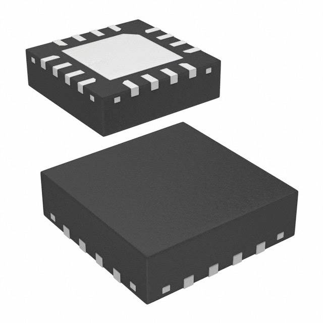
- Part No.:
- ADP5090ACPZ-1-R7
- Manufacturer:
- Analog Devices Inc.
- Category:
- Battery Chargers
- Package:
- 16-WFQFN Exposed Pad, CSP
- Datasheet:
-
 ADP5090ACPZ-1-R7.pdf
- Description:
- IC BATT CHG MULTI-CHEM 16LFCSP
- Quantity:
- Payment:

- Shipping:

Inventory:1,241
Please send an inquiry. Send us your inquiry, and we will respond immediately.
Product details
Overview
ADP5090ACPZ-1-R7 from Analog Devices is an ultralow power boost regulator with integrated MPPT, charge management, and power path control for energy harvesting systems. It operates from 80 mV to 3.3 V input, delivers up to 800 mA at BAT, supports cold start from 380 mV, and features 320 nA quiescent current (CBP ≥ MINOP) - enabling self-powered wireless sensor nodes powered by PV cells or TEGs.
For engineers reviewing the ADP5090ACPZ-1-R7 datasheet, ADP5090ACPZ-1-R7 pinout, ADP5090ACPZ-1-R7 application, or ADP5090ACPZ-1-R7 equivalent, key selection criteria include cold-start capability, programmable MPPT ratio, battery overcharge/discharge thresholds, PGOOD flag behavior, and backup primary cell integration via BACK_UP pin.
Technical Context
The ADP5090ACPZ-1-R7 implements a hysteretic synchronous boost controller with integrated high-side and low-side MOSFETs (RHS_DS_ON = 1.38 Ω typ, RLS_DS_ON = 1.25 Ω typ), operating in pulse frequency mode (PFM) for sub-µW efficiency at ultralight loads. Its MPPT loop samples VIN open-circuit voltage every 19 s and holds it on CBP using a 10 nF capacitor to maintain operation at peak harvest power.
Energy storage management includes dual-threshold battery protection (VBAT_TERM = 2.2–5.2 V programmable, VBAT_SD = 2 V fixed), SYS-switch on-resistance of 0.48 Ω, and automatic power path arbitration between harvested energy, rechargeable storage (BAT), and optional primary cell (BACK_UP), with 185 mV comparator offset preventing backfeed.
Key Specifications
| Parameter | Value and Actual Design Meaning |
|---|---|
| Cold-start input voltage | 380 mV typical - enables startup from weak photovoltaic or thermoelectric sources before system voltage builds |
| Input voltage range (post-cold-start) | 80 mV to 3.3 V - supports ultra-low-voltage energy harvesters including micro-PV and low-ΔT TEGs |
| Quiescent current (active) | 320 nA typical (CBP ≥ MINOP) - minimizes drain during intermittent light/heat conditions |
| MPPT sampling cycle | 19 s interval with 296 ms sampling window - balances tracking accuracy against system interruption time |
| Battery charge termination | Programmable 2.2 V to 5.2 V - matches Li-ion, thin-film, or supercapacitor voltage profiles |
| SYS switch on-resistance | 0.48 Ω typical - limits voltage drop under 800 mA load, preserving system rail stability |
| Backup path comparator offset | 185 mV typical - prevents BACK_UP pin from being charged by BAT or SYS, ensuring unidirectional flow |
Pinout & Package
The ADP5090ACPZ-1-R7 is housed in a 16-lead, 3 mm × 3 mm LFCSP package with exposed pad connected to AGND. Thermal resistance θJA = 53.1°C/W enables operation up to +125°C junction temperature.
| Pin/Terminal | Circuit Role | Design Meaning |
|---|---|---|
| SETSD | Battery discharge shutdown threshold input | Resistor divider sets fixed 2 V shutdown point - prevents deep discharge of Li-ion or thin-film batteries |
| TERM | Battery charge termination voltage input | Resistor divider programs 2.2–5.2 V cutoff - configurable for diverse storage chemistries |
| MINOP | Minimum operating power enable/disable | Resistor sets input voltage threshold; grounding disables MPPT and reduces IQ to 260 nA |
| MPPT | Maximum Power Point Tracking ratio setting | Resistor divider defines OCV scaling (e.g., 80% for PV, 50% for TEG) - determines optimal harvest point |
| CBP | MPPT reference hold capacitor node | 10 nF capacitor stores sampled OCV - maintains regulation reference between 19 s sampling intervals |
| DIS_SW | Boost regulator disable control | Logic-high signal halts switching within 1 µs - eliminates RF interference during transmission bursts |
| BACK_UP | Primary cell backup supply input | Enables automatic switchover when SYS drops below BAT; 400 mA capability with inrush limiting |
| PGOOD | System voltage status flag output | Open-drain logic-high when SYS > SETPG threshold - signals MCU that regulated rail is stable |
Key Features
| Feature | Design Value |
|---|---|
| Cold-start circuit with charge pump | Starts regulation from 380 mV input without external assistance - eliminates need for precharged storage |
| Hysteretic PFM boost control | Maintains >70% efficiency at 10 µA input current - critical for microwatt-level ambient energy sources |
| Programmable MPPT ratio | Supports both PV (≈80%) and TEG (≈50%) harvesters via resistor divider - avoids redesign across transducer types |
| Triple-source power path | Automatically selects among harvester, rechargeable storage (BAT), and primary cell (BACK_UP) - ensures continuous uptime |
| RF-friendly DIS_SW pin | Sub-microsecond disable/enable timing - synchronizes boost shutdown with wireless TX windows to avoid spectral contamination |
Applications
| Photovoltaic Energy Harvesting | Thermoelectric Energy Harvesting |
|---|---|
Use Scenario: Indoor solar-powered environmental sensor node harvesting from low-light amorphous PV panels. IC Role / Device Role / Timing Role: Primary power manager converting 0.2–1.2 V PV output into stable 3.3 V SYS rail while maximizing harvest via OCV-sampled MPPT. Use Value: Enables multi-year battery-free operation using only ambient light, with cold-start from 380 mV eliminating need for initial charge. | Use Scenario: Industrial pipe-monitoring node harvesting waste heat via TEG mounted on steam lines. IC Role / Device Role / Timing Role: Ultralow-input boost regulator managing 80–500 mV TEG output, with MPPT ratio set to 50% for optimal ΔT-based power extraction. Use Value: Sustains 2.4 GHz RF transmission cycles using only thermal gradients, with 260 nA sleep current extending maintenance intervals. |
| Wireless Sensor Node Power Management | Industrial Battery-Free Monitoring |
Use Scenario: LoRaWAN soil moisture sensor deployed in shaded agricultural fields with intermittent light exposure. IC Role / Device Role / Timing Role: Energy-aware power hub managing charge/discharge of supercapacitor (BAT), PGOOD-triggered MCU wake-up, and DIS_SW-synchronized RF transmit. Use Value: Eliminates primary batteries by combining cold-start, programmable shutdown (MINOP), and RF-transparent boost control - reducing lifetime cost and environmental impact. | Use Scenario: Predictive maintenance vibration sensor on rotating machinery with no accessible power source. IC Role / Device Role / Timing Role: Triple-path power arbitrator selecting between TEG harvest, supercapacitor storage, and CR2032 backup (BACK_UP) during extended downtime. Use Value: Guarantees data continuity during zero-harvest periods via seamless backup switchover - no firmware intervention required. |
Equivalent & Alternatives
The following parts are listed as comparable options for similar energy harvesting power management applications.
| Alternative Part | Technical Difference | Application Difference | Selection Advice |
|---|---|---|---|
| LTC3331IDHD#PBF | Integrated buck-boost + AC/DC piezoelectric input; higher 680 nA IQ; no MPPT; 20 V max input | Better suited for piezoelectric or AC harvesters; lacks OCV-sampling MPPT for PV/TEG optimization | Select when harvesting from vibration or AC sources; avoid for PV/TEG where MPPT is essential |
| BQ25504RGTT | Lower 330 nA IQ; 150 mV cold-start; no BACK_UP path; 5.5 V max SYS; no DIS_SW pin | Optimized for ultra-low-power PV-only use; lacks primary-cell backup and RF-synchronization capability | Select for cost-sensitive, single-source PV designs without RF coexistence requirements |
Compared with LTC3331IDHD#PBF and BQ25504RGTT, the ADP5090ACPZ-1-R7 uniquely combines cold-start from 380 mV, programmable MPPT for both PV and TEG, and a dedicated RF-friendly DIS_SW pin - making it the only option supporting robust, multi-source, wireless-integrated energy harvesting in industrial environments.
Availability
ADP5090ACPZ-1-R7 is available at Aetrix Electronics and suitable for photovoltaic energy harvesting, thermoelectric generator systems, and battery-free wireless sensor networks requiring stable component supply across automotive-grade temperature ranges and long-lifecycle deployments.
Supply support for ADP5090ACPZ-1-R7 includes scheduled delivery planning, volume procurement assistance, BOM continuity management, traceable sourcing, and lifecycle availability coordination for OEM customers, industrial embedded developers, connected-device designers, and electronics production programs.
Manufacturer
Analog Devices is a global leader in high-performance analog, mixed-signal, and digital signal processing semiconductors, serving precision instrumentation, industrial automation, and energy-efficient systems.
The ADP5090ACPZ-1-R7 belongs to Analog Devices' energy harvesting PMIC product line, engineered specifically to enable maintenance-free, battery-free operation of IoT edge sensors by maximizing microwatt-level ambient energy conversion.
FAQ
What is the minimum input voltage required for cold-start operation of the ADP5090ACPZ-1-R7?
The ADP5090ACPZ-1-R7 achieves cold-start operation from a minimum input voltage of 380 mV (typical) at the VIN pin when the SYS voltage is below 1.93 V. This capability is enabled by an internal charge-pump circuit and allows the ADP5090ACPZ-1-R7 to begin regulation even when no stored energy is present - critical for deploying truly battery-free systems powered solely by ambient light or heat.
How does the MPPT function work in the ADP5090ACPZ-1-R7, and what harvester types does it support?
The ADP5090ACPZ-1-R7 implements MPPT by periodically sampling the VIN open-circuit voltage (every 19 s for 296 ms), scaling it via a resistor divider at the MPPT pin, and holding the result on the CBP capacitor. This allows the boost regulator to operate at the input voltage corresponding to maximum power extraction. The ADP5090ACPZ-1-R7 supports both photovoltaic cells (MPPT ratio ≈ 80%) and thermoelectric generators (MPPT ratio ≈ 50%), with the ratio set externally - no firmware or calibration required.
Can the ADP5090ACPZ-1-R7 manage multiple energy storage elements simultaneously?
Yes, the ADP5090ACPZ-1-R7 manages three distinct power domains: harvested input (VIN), rechargeable storage (BAT), and optional primary-cell backup (BACK_UP). It autonomously arbitrates between them using internal comparators and power switches - for example, sourcing from BACK_UP when SYS falls below VSYS_TH and BAT is depleted. The ADP5090ACPZ-1-R7 does not require external logic to coordinate these paths, simplifying system architecture.
What is the purpose of the DIS_SW pin on the ADP5090ACPZ-1-R7, and how fast does it respond?
The DIS_SW pin on the ADP5090ACPZ-1-R7 provides hardware-level, RF-friendly control to temporarily halt boost switching - preventing electromagnetic interference during wireless transmission. Driving DIS_SW high disables the regulator within 1 µs (typical), and pulling it low resumes operation immediately. This feature is integral to the ADP5090ACPZ-1-R7's design for coexistence with 2.4 GHz BLE or sub-GHz LoRa radios in compact sensor nodes.
How is battery overcharge protection implemented in the ADP5090ACPZ-1-R7?
Battery overcharge protection in the ADP5090ACPZ-1-R7 is implemented via the TERM pin: an external resistor divider sets the VBAT_TERM threshold between 2.2 V and 5.2 V. When the BAT voltage exceeds this threshold, the ADP5090ACPZ-1-R7 disables the boost regulator. Hysteresis (3.7% typical) prevents oscillation, and regulation resumes only after BAT falls below VBAT_TERM_HYS. This fully hardware-based protection requires no MCU intervention and applies directly to the ADP5090ACPZ-1-R7's integrated charge control block.
ADP5090ACPZ-1-R7 Specifications
- Product attributes
- Attribute value
- Manufacturer:
- Analog Devices Inc.
- Series:
- -
- Package/Case:
- 16-WFQFN Exposed Pad, CSP
- Packaging:
- Tape & Reel (TR)
- Product Status:
- Active
- Battery Chemistry:
- Multi-Chemistry
- Number of Cells:
- -
- Current - Charging:
- -
- Programmable Features:
- Voltage
- Fault Protection:
- Over Current, Over Temperature, Short Circuit
- Charge Current - Max:
- -
- Battery Pack Voltage:
- -
- Voltage - Supply (Max):
- 3.3V
- Interface:
- -
- Operating Temperature:
- -40°C ~ 125°C (TJ)
- Grade:
- -
- Qualification:
- -
- Mounting Type:
- Surface Mount
- Supplier Device Package:
- 16-LFCSP-WQ (3x3)
ADP5090ACPZ-1-R7 FAQ
1.How can I place an order for ADP5090ACPZ-1-R7 through Aetrix?
Please submit a Request for Quotation (RFQ) for ADP5090ACPZ-1-R7 on Aetrix. Our sales agent will provide a competitive quotation and guide you through the order confirmation once you accept the terms.
2.Are the price and stock information for ADP5090ACPZ-1-R7 reliable?
The price and inventory of ADP5090ACPZ-1-R7 are updated periodically and may fluctuate due to market conditions. Stock and pricing data are typically refreshed every 24 hours. Quotation validity for ADP5090ACPZ-1-R7 is usually 5 days.
3.What payment methods are accepted for ADP5090ACPZ-1-R7?
We accept Wire Transfer, PayPal, Credit Card, Western Union, MoneyGram, and Escrow for ADP5090ACPZ-1-R7 transactions.
Note: Certain payment methods may incur a processing fee.
4.How is shipping managed for ADP5090ACPZ-1-R7?
ADP5090ACPZ-1-R7 orders can be shipped via leading logistics carriers, including DHL, UPS, FedEx, TNT, or Registered Mail.
Once your ADP5090ACPZ-1-R7 order is processed, you will receive an email with the shipment details and tracking number.
Note: Tracking information may take up to 24 hours to appear. Express delivery typically takes 3–5 business days.
5.How can I obtain technical support or documentation for ADP5090ACPZ-1-R7?
For technical support, including ADP5090ACPZ-1-R7 datasheets, pinout diagrams, or application guidance, please contact our engineering support team. They can provide detailed documentation and assistance for your ADP5090ACPZ-1-R7 requirements.
6.How does Aetrix verify that ADP5090ACPZ-1-R7 is sourced from the original manufacturer or authorized distributors?
All ADP5090ACPZ-1-R7 products on Aetrix are procured from qualified distributors and authorized channels. Our dedicated quality assurance team conducts strict verification, including traceability checks and, if necessary, third-party testing. This ensures that ADP5090ACPZ-1-R7 meets industry standards.
7.What is the process for return or replacement of ADP5090ACPZ-1-R7?
All ADP5090ACPZ-1-R7 units undergo pre-shipment inspection (PSI). If there is an issue with ADP5090ACPZ-1-R7, returns or replacements are accepted under the following conditions:
1.Quantity discrepancies, incorrect items, or visible external defects (such as breakage or corrosion), acknowledged by Aetrix.
2.The issue is reported within 90 days of delivery.
3.The ADP5090ACPZ-1-R7 part is unused and in its original packaging.
Return procedure for ADP5090ACPZ-1-R7:
1.Submit a request within 90 days.
2.Obtain a Return Material Authorization (RMA) from Aetrix.
ADP5090ACPZ-1-R7 Tags

-
BQ21040DBVR
Texas Instruments

-
MCP73812T-420I/OT
Microchip Technology
-
MCP73831T-2ACI/OT
Microchip Technology
-
MCP73832T-2ACI/OT
Microchip Technology
-
MCP73831T-2DCI/OT
Microchip Technology
-
MCP73832T-2DCI/OT
Microchip Technology
-
MCP73831T-2ATI/OT
Microchip Technology
-
MCP73832T-2ATI/OT
Microchip Technology
-
MCP73831T-5ACI/OT
Microchip Technology

-
MCP73832T-2ACI/MC
Microchip Technology
-
MCP73831T-2ACI/MC
Microchip Technology
-
MCP73831T-2ATI/MC
Microchip Technology
Tech Hub

A practical engineering guide to 3.3V and 5V logic compatibility, input thresholds, resistor dividers, translator ICs, MOSFET level shifting, I2C pull-ups, timing limits and power-sequencing risks.

The 74HC595 uses push-pull logic outputs, while the TPIC6B595 uses 50 V open-drain DMOS sinks for higher-power loads. This guide compares timing, current limits, 3.3 V interfacing, load wiring, thermal…

The 74HC595 converts serial data into eight stable parallel outputs. This guide covers pin functions, shift and storage timing, OE and MR behavior, drive-current limits, cascading, voltage compatibilit…

A technical comparison of level-sensitive latches and edge-triggered flip-flops, covering timing windows, setup and hold limits, master–slave operation, time borrowing, race-through, HDL inference and…

A D latch stores one bit while Enable controls when data can pass. This reference covers gate-level operation, truth tables, transparency, setup and hold timing, LE versus OE, common ICs and practical …

An SR latch stores one bit through cross-coupled feedback. This engineering reference covers NOR and NAND implementations, truth tables, forbidden-state recovery, gated operation, switch debouncing, fa…

Latch circuits retain one bit through feedback. This technical reference covers SR and D latches, truth tables, transparency, timing limits, latch-versus-flip-flop behavior, applications and common log…

An engineering guide to LED driver operation, constant-current and constant-voltage outputs, linear and switching topologies, dimming, IC selection, calculations, replacement compatibility, and fault c…

Operational amplifier guide covering op amp basics, feedback, ideal vs real op amps, common configurations, buffer circuits, offset, bias current, gain-bandwidth, slew rate, rail-to-rail limits and sel…

Jumper cables guide covering safe connection order, red and black clamp placement, final ground connection, cable gauge, length, clamp quality, copper vs CCA cables, jump starter comparison and battery…


