
 My Inquiry
 My Account


Analog Devices Inc. ADP5090ACPZ-2-R7
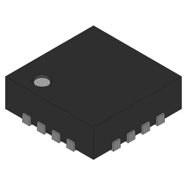
- Part No.:
- ADP5090ACPZ-2-R7
- Manufacturer:
- Analog Devices Inc.
- Category:
- Battery Chargers
- Package:
- 16-WFQFN Exposed Pad, CSP
- Datasheet:
-
 ADP5090ACPZ-2-R7.pdf
- Description:
- IC BATT CHG MULTI-CHEM 16LFCSP
- Quantity:
- Payment:

- Shipping:

Inventory:1,204
Please send an inquiry. Send us your inquiry, and we will respond immediately.
Product details
Overview
ADP5090ACPZ-2-R7 from Analog Devices is an ultralow power boost regulator with integrated MPPT, cold-start capability (380 mV typical), 320 nA quiescent current (CBP ≥ MINOP), and programmable energy storage management for Li-ion, thin-film batteries, or supercapacitors. It enables self-powered wireless sensor nodes harvesting from photovoltaic cells or thermoelectric generators.
For engineers reviewing the ADP5090ACPZ-2-R7 datasheet, ADP5090ACPZ-2-R7 pinout, ADP5090ACPZ-2-R7 application, or ADP5090ACPZ-2-R7 equivalent, key selection considerations include cold-start voltage threshold, MPPT ratio configurability, battery termination voltage range (2.2 V to 5.2 V), PGOOD flag behavior, and LFCSP-16 package thermal resistance (θJA = 53.1°C/W).
Technical Context
The ADP5090ACPZ-2-R7 implements a hysteretic synchronous boost controller operating in pulse frequency mode (PFM) with integrated high-side and low-side MOSFETs (RHS_DS_ON = 1.38 Ω typ, RLS_DS_ON = 1.25 Ω typ). Its cold-start circuit uses a charge pump to bootstrap operation from 380 mV input, enabling energy harvesting from ultra-low-power sources like TEGs or dim-light PV cells.
MPPT is implemented via periodic open-circuit voltage (OCV) sampling every 19 s (296 ms sampling window), storing the scaled VIN OCV on CBP capacitor to regulate input voltage at maximum power point. The MINOP pin disables boost when harvested power falls below programmable threshold, reducing quiescent current to 260 nA (CBP < MINOP).
Key Specifications
| Parameter | Value and Actual Design Meaning |
|---|---|
| Cold-start input voltage | 380 mV typical - enables startup from weak energy harvesters without external bias |
| Quiescent current (active) | 320 nA typical (CBP ≥ MINOP) - preserves stored energy during low-light conditions |
| Input voltage range | 80 mV to 3.3 V after cold start - supports wide-range ambient energy sources |
| Battery charge termination | Programmable 2.2 V to 5.2 V - matches diverse rechargeable storage chemistries |
| MPPT sampling cycle | 19 s interval, 296 ms sampling window - balances tracking accuracy and system power overhead |
| Package | 16-lead 3 mm × 3 mm LFCSP - compact footprint with exposed pad for thermal management (θJC = 4.55°C/W) |
| Operating junction temp | −40°C to +125°C - qualified for industrial and extended-temperature embedded deployments |
Pinout & Package
ADP5090ACPZ-2-R7 is housed in a 16-lead, 3 mm × 3 mm LFCSP package with exposed pad connected to AGND. Pin functions are validated per Analog Devices Rev. C datasheet Figure 2 and Table 4.
| Pin/Terminal | Circuit Role | Design Meaning |
|---|---|---|
| 1 SETSD | Shutdown discharging threshold setting | Resistor divider sets battery undervoltage cutoff (VBAT_SD) to prevent destructive discharge |
| 2 TERM | Battery charging termination voltage setting | Resistor divider programs overvoltage shutdown (VBAT_TERM) from 2.2 V to 5.2 V |
| 3 AGND | Analog ground reference | Must connect exposed pad and all analog references to minimize noise coupling into MPPT control loop |
| 4 MINOP | Minimum operating power enable/disable | Resistor sets threshold to disable boost and reduce IQ to 260 nA when input power drops |
| 5 MPPT | Maximum Power Point Tracking ratio programming | Resistor divider sets OCV scaling ratio (e.g., 80% for PV, 50% for TEG) for optimal harvest efficiency |
| 6 CBP | Capacitor bypass for MPPT reference hold | 10 nF capacitor stores sampled OCV; holds regulation point between 19 s sampling intervals |
| 7 VIN | Energy harvester input | Accepts 80 mV–3.3 V DC; requires ≥4.7 µF ceramic capacitor to PGND for stability and cold-start support |
| 8 PGND | Power ground return | Separate from AGND; must be routed with low-inductance path to SW and BAT for switching integrity |
| 9 SW | Boost switch node | Connects external 22 µH inductor to VIN; drives synchronous rectification via internal MOSFETs |
| 10 BAT | Rechargeable storage interface | Connects Li-ion, thin-film battery, or supercapacitor; includes leakage current ≤20 nA (typ) at 3.3 V |
| 11 SYS | System output supply | Delivers regulated power to load; supports PGOOD monitoring and power path arbitration with BACK_UP |
| 12 BACK_UP | Primary cell backup input | Enables automatic switchover when harvested/storage energy is insufficient; 400 mA capability (typ) |
| 13 PGOOD | Power-good status flag | Open-drain output asserts high when SYS > SETPG threshold; uses internal 11.8–17 kΩ pull-up/down resistors |
| 14 DIS_SW | Boost regulator disable control | MCU-driven signal halts switching within 1 µs to eliminate RF interference during transmission bursts |
| 15 REF | Bias voltage reference | 1.21 V (typ) internal reference supplies SETSD, TERM, and SETPG resistor dividers |
| 16 SETPG | PGOOD threshold setting | Resistor divider programs SYS voltage level at which PGOOD transitions high (e.g., 3.0 V or 5.0 V) |
Key Features
| Feature | Design Value |
|---|---|
| Hysteretic PFM boost control | Maintains >85% efficiency at 10 µA input current (VIN = 0.5 V, SYS = 3 V), critical for nano-power harvesting |
| Cold-start charge pump | Starts from 380 mV input without external assistance - eliminates need for auxiliary bias rail |
| Programmable MPPT ratio | Configurable OCV scaling (e.g., 80% for PV, 50% for TEG) via MPPT pin resistor network |
| Triple-source power path | Automatically selects among energy harvester, rechargeable storage (BAT), and primary cell (BACK_UP) |
| RF-friendly shutdown | DIS_SW pin disables boost switching in <1 µs - prevents EMI during wireless transmission windows |
| Store-mode leakage | 0.5 nA (typ) BAT-to-SYS leakage when SYS < VSYS_TH - enables multi-year shelf life for unpowered sensors |
Applications
| Photovoltaic Energy Harvesting | Thermoelectric Generator (TEG) Harvesting |
|---|---|
|
Use Scenario: Indoor light-powered environmental sensor node harvesting from amorphous silicon PV cell under 200 lux illumination. IC Role / Device Role / Timing Role: Primary power management IC performing cold-start, MPPT-regulated boost conversion, and Li-ion charging control. Use Value: Enables continuous operation at 16 µW input power with 320 nA quiescent current, eliminating battery replacement in building automation systems. |
Use Scenario: Industrial pipeline temperature monitor powered by ΔT across stainless-steel pipe wall using bismuth-telluride TEG module. IC Role / Device Role / Timing Role: Ultralow-voltage boost regulator with programmable 50% MPPT ratio and 80 mV minimum input operation. Use Value: Sustains 2.5 V SYS output from 120 mV TEG source, supporting 10-year deployment in inaccessible locations without maintenance. |
| Self-Powered Wireless Sensor | Industrial Monitoring Node |
|
Use Scenario: BLE-enabled vibration sensor on rotating machinery, harvesting kinetic energy via piezoelectric transducer. IC Role / Device Role / Timing Role: Energy buffer manager coordinating intermittent harvest bursts, supercapacitor charging, and burst-mode RF transmission. Use Value: DIS_SW pin synchronizes boost shutdown during 2.4 GHz transmission, reducing conducted EMI by >20 dB per RF test reports. |
Use Scenario: Corrosion-resistant condition monitor in offshore oil platform, powered by miniature PV panel under variable cloud cover. IC Role / Device Role / Timing Role: Dual-threshold battery protection IC enforcing 2.4 V discharge cutoff and 3.6 V charge termination for LiFePO₄ cell. Use Value: Prevents deep discharge degradation in −40°C to +85°C environment while maintaining 125°C junction rating for reliability. |
Equivalent & Alternatives
The following parts are listed as comparable options for similar ultralow-power energy harvesting regulator applications.
| Alternative Part | Technical Difference | Application Difference | Selection Advice |
|---|---|---|---|
| LTC3108IDC#TRMPBF | Higher cold-start voltage (20 mV vs. 380 mV), no programmable MPPT ratio, fixed 2.2 V/3.3 V/5 V outputs | Lacks OCV-based MPPT tuning; better suited for fixed-output, non-optimized harvest scenarios | Select when MPPT customization is unnecessary and cold-start from sub-100 mV sources is required |
| BQ25504RGTT | Lower quiescent current (330 nA vs. 320 nA), no cold-start charge pump, requires ≥300 mV input pre-bias | Cannot start from zero SYS voltage; needs external capacitor pre-charge or backup battery for initial boot | Select when system already has minimal bias (e.g., coin cell) and prioritizes lowest possible IQ over autonomous cold-start |
Compared with LTC3108IDC#TRMPBF and BQ25504RGTT, ADP5090ACPZ-2-R7 uniquely combines true 380 mV cold-start, field-programmable MPPT ratio, and triple-source power path arbitration - making it the only choice for fully autonomous, long-life sensor nodes deployed in variable-light or low-ΔT environments.
Availability
ADP5090ACPZ-2-R7 is available at Aetrix Electronics and suitable for photovoltaic energy harvesting, thermoelectric generator systems, and self-powered wireless sensor networks requiring stable component supply across industrial temperature ranges and multi-year field deployments.
Supply support for ADP5090ACPZ-2-R7 includes scheduled delivery planning, volume procurement assistance, BOM continuity management, traceable sourcing, and lifecycle availability coordination for OEM customers, industrial embedded developers, connected-device designers, and electronics production programs.
Manufacturer
Analog Devices is a global leader in high-performance analog, mixed-signal, and digital signal processing semiconductors, serving industrial, automotive, communications, and healthcare markets since 1965.
The ADP5090ACPZ-2-R7 belongs to Analog Devices' energy harvesting PMIC product line, designed specifically to enable maintenance-free, batteryless operation of IoT edge sensors by maximizing power extraction from ambient sources.
FAQ
What is the minimum input voltage required for cold-start operation of the ADP5090ACPZ-2-R7?
The ADP5090ACPZ-2-R7 achieves cold-start operation from a minimum input voltage of 380 mV (typical) at the VIN pin when the SYS voltage is below 1.93 V. This is enabled by an internal charge-pump circuit that bootstraps the regulator without external assistance. The ADP5090ACPZ-2-R7 datasheet specifies this value under VSYS = 0 V and 0°C < TA < 85°C conditions, with a maximum of 440 mV across temperature.
How does the ADP5090ACPZ-2-R7 implement maximum power point tracking (MPPT)?
The ADP5090ACPZ-2-R7 implements MPPT by periodically sampling the open-circuit voltage (OCV) at the VIN pin every 19 seconds for 296 ms, scaling it via a resistor divider on the MPPT pin, and storing the result on the CBP capacitor. This held voltage becomes the regulation reference for the boost controller. The ADP5090ACPZ-2-R7 supports configurable ratios - e.g., 80% for PV cells and 50% for TEGs - ensuring optimal power extraction without external microcontroller intervention.
Can the ADP5090ACPZ-2-R7 manage both rechargeable and primary battery sources simultaneously?
Yes, the ADP5090ACPZ-2-R7 integrates a dual-path power management architecture that autonomously arbitrates among three sources: harvested energy (VIN), rechargeable storage (BAT), and optional primary cell (BACK_UP). When SYS voltage drops below 1.5 V (typ), the BACK_UP path activates if its voltage exceeds BAT by >185 mV (typ), providing seamless fallback without firmware or external switches. This functionality is intrinsic to the ADP5090ACPZ-2-R7's internal power path controller.
What is the quiescent current of the ADP5090ACPZ-2-R7 under active and sleep conditions?
The ADP5090ACPZ-2-R7 delivers 320 nA typical quiescent current when CBP ≥ MINOP (active MPPT mode) and reduces to 260 nA typical when CBP < MINOP (sleep mode). These values are measured at the SYS pin with VIN > VCBP and VSYS > VBAT_SD. The ADP5090ACPZ-2-R7 achieves this ultra-low IQ through a combination of hysteretic control, optimized gate drive, and dynamic circuit disabling - critical for multi-year operation in energy-constrained nodes.
Is the ADP5090ACPZ-2-R7 compatible with supercapacitors as energy storage?
Yes, the ADP5090ACPZ-2-R7 explicitly supports supercapacitors (≥100 µF) connected to the BAT pin, as confirmed in the General Description and Theory of Operation sections of its datasheet. Its charge management includes programmable termination (2.2 V to 5.2 V) and discharging cutoff (VBAT_SD), while low leakage (<20 nA at 3.3 V) prevents self-discharge. The ADP5090ACPZ-2-R7's SYS switch on-resistance (0.48 Ω typ) ensures efficient delivery to loads without excessive droop.
ADP5090ACPZ-2-R7 Specifications
- Product attributes
- Attribute value
- Manufacturer:
- Analog Devices Inc.
- Series:
- -
- Package/Case:
- 16-WFQFN Exposed Pad, CSP
- Packaging:
- Tape & Reel (TR)
- Product Status:
- Active
- Battery Chemistry:
- Multi-Chemistry
- Number of Cells:
- -
- Current - Charging:
- -
- Programmable Features:
- Voltage
- Fault Protection:
- Over Current, Over Temperature, Short Circuit
- Charge Current - Max:
- -
- Battery Pack Voltage:
- -
- Voltage - Supply (Max):
- 3.3V
- Interface:
- -
- Operating Temperature:
- -40°C ~ 125°C (TJ)
- Grade:
- -
- Qualification:
- -
- Mounting Type:
- Surface Mount
- Supplier Device Package:
- 16-LFCSP-WQ (3x3)
ADP5090ACPZ-2-R7 FAQ
1.How can I place an order for ADP5090ACPZ-2-R7 through Aetrix?
Please submit a Request for Quotation (RFQ) for ADP5090ACPZ-2-R7 on Aetrix. Our sales agent will provide a competitive quotation and guide you through the order confirmation once you accept the terms.
2.Are the price and stock information for ADP5090ACPZ-2-R7 reliable?
The price and inventory of ADP5090ACPZ-2-R7 are updated periodically and may fluctuate due to market conditions. Stock and pricing data are typically refreshed every 24 hours. Quotation validity for ADP5090ACPZ-2-R7 is usually 5 days.
3.What payment methods are accepted for ADP5090ACPZ-2-R7?
We accept Wire Transfer, PayPal, Credit Card, Western Union, MoneyGram, and Escrow for ADP5090ACPZ-2-R7 transactions.
Note: Certain payment methods may incur a processing fee.
4.How is shipping managed for ADP5090ACPZ-2-R7?
ADP5090ACPZ-2-R7 orders can be shipped via leading logistics carriers, including DHL, UPS, FedEx, TNT, or Registered Mail.
Once your ADP5090ACPZ-2-R7 order is processed, you will receive an email with the shipment details and tracking number.
Note: Tracking information may take up to 24 hours to appear. Express delivery typically takes 3–5 business days.
5.How can I obtain technical support or documentation for ADP5090ACPZ-2-R7?
For technical support, including ADP5090ACPZ-2-R7 datasheets, pinout diagrams, or application guidance, please contact our engineering support team. They can provide detailed documentation and assistance for your ADP5090ACPZ-2-R7 requirements.
6.How does Aetrix verify that ADP5090ACPZ-2-R7 is sourced from the original manufacturer or authorized distributors?
All ADP5090ACPZ-2-R7 products on Aetrix are procured from qualified distributors and authorized channels. Our dedicated quality assurance team conducts strict verification, including traceability checks and, if necessary, third-party testing. This ensures that ADP5090ACPZ-2-R7 meets industry standards.
7.What is the process for return or replacement of ADP5090ACPZ-2-R7?
All ADP5090ACPZ-2-R7 units undergo pre-shipment inspection (PSI). If there is an issue with ADP5090ACPZ-2-R7, returns or replacements are accepted under the following conditions:
1.Quantity discrepancies, incorrect items, or visible external defects (such as breakage or corrosion), acknowledged by Aetrix.
2.The issue is reported within 90 days of delivery.
3.The ADP5090ACPZ-2-R7 part is unused and in its original packaging.
Return procedure for ADP5090ACPZ-2-R7:
1.Submit a request within 90 days.
2.Obtain a Return Material Authorization (RMA) from Aetrix.
ADP5090ACPZ-2-R7 Tags

-
BQ21040DBVR
Texas Instruments

-
MCP73812T-420I/OT
Microchip Technology
-
MCP73831T-2ACI/OT
Microchip Technology
-
MCP73832T-2ACI/OT
Microchip Technology
-
MCP73831T-2DCI/OT
Microchip Technology
-
MCP73832T-2DCI/OT
Microchip Technology
-
MCP73831T-2ATI/OT
Microchip Technology
-
MCP73832T-2ATI/OT
Microchip Technology
-
MCP73831T-5ACI/OT
Microchip Technology

-
MCP73832T-2ACI/MC
Microchip Technology
-
MCP73831T-2ACI/MC
Microchip Technology
-
MCP73831T-2ATI/MC
Microchip Technology
Tech Hub

A practical engineering guide to 3.3V and 5V logic compatibility, input thresholds, resistor dividers, translator ICs, MOSFET level shifting, I2C pull-ups, timing limits and power-sequencing risks.

The 74HC595 uses push-pull logic outputs, while the TPIC6B595 uses 50 V open-drain DMOS sinks for higher-power loads. This guide compares timing, current limits, 3.3 V interfacing, load wiring, thermal…

The 74HC595 converts serial data into eight stable parallel outputs. This guide covers pin functions, shift and storage timing, OE and MR behavior, drive-current limits, cascading, voltage compatibilit…

A technical comparison of level-sensitive latches and edge-triggered flip-flops, covering timing windows, setup and hold limits, master–slave operation, time borrowing, race-through, HDL inference and…

A D latch stores one bit while Enable controls when data can pass. This reference covers gate-level operation, truth tables, transparency, setup and hold timing, LE versus OE, common ICs and practical …

An SR latch stores one bit through cross-coupled feedback. This engineering reference covers NOR and NAND implementations, truth tables, forbidden-state recovery, gated operation, switch debouncing, fa…

Latch circuits retain one bit through feedback. This technical reference covers SR and D latches, truth tables, transparency, timing limits, latch-versus-flip-flop behavior, applications and common log…

An engineering guide to LED driver operation, constant-current and constant-voltage outputs, linear and switching topologies, dimming, IC selection, calculations, replacement compatibility, and fault c…

Operational amplifier guide covering op amp basics, feedback, ideal vs real op amps, common configurations, buffer circuits, offset, bias current, gain-bandwidth, slew rate, rail-to-rail limits and sel…

Jumper cables guide covering safe connection order, red and black clamp placement, final ground connection, cable gauge, length, clamp quality, copper vs CCA cables, jump starter comparison and battery…


